3 application function i/o (afi), 4 timing specifications – ADLINK PCIe-7360 User Manual
Page 14
4
Introduction
1.3.3
Application Function I/O (AFI)
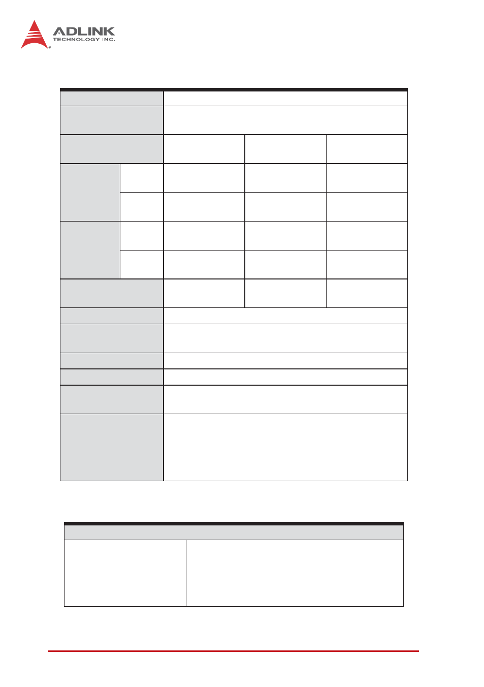
1.3.4
Timing Specifications
Channels
8
Direction
(programmable)
Input or output, per channel basis
Logic levels
(programmable)
1.8 V
2.5 V
3.3 V (5 V
compatible)
Input
voltage
Min.
V
IH
1.2 V
1.6 V
2 V
Max.
V
IL
0.63 V
0.7 V
0.8 V
Output
voltage
Min.
V
OH
1.6 V
2.3 V
3.1 V
Max.
V
OL
0.2 V
0.2 V
0.2 V
Driving capacity
(max.)
±8 mA
±16 mA
±32 mA
Input impedance
10 kΩ
Input protection
range
-1 to 6 V
Output impedance
50 Ω
Power-up initial state Tri-state/All digital inputs
Output protection
range
-0.5V to 3.8V
Supported Modes
(programmable)
I
2
C master
SPI master
Handshake
External trigger in/out
DI/DO sample clock in/out
Sample Clock
Clock sources
Internal clock: onboard 100MHz with 16-bit
divider
External clock: AFI6 (for DO)
AFI7 (for DI)
SMB CLK in
- USB-1901 (84 pages)
- USB-1210 (54 pages)
- USB-2401 (60 pages)
- USB-7230 (50 pages)
- USB-2405 (56 pages)
- DAQe-2010 (92 pages)
- DAQe-2204 (100 pages)
- DAQe-2213 (94 pages)
- DAQe-2501 (74 pages)
- PXI-2010 (84 pages)
- PXI-2020 (60 pages)
- PXI-2501 (62 pages)
- cPCI-9116 (98 pages)
- ACL-8112 Series (93 pages)
- ACL-8112 Series (94 pages)
- ACL-8112 Series (92 pages)
- ACL-8216 (75 pages)
- ACL-8111 (61 pages)
- PCM-9112+ (94 pages)
- PCM-9112+ (10 pages)
- cPCI-6216V (47 pages)
- ACL-6126 (28 pages)
- ACL-6128A (40 pages)
- PCM-6308V+ (52 pages)
- PCM-6308V+ (4 pages)
- PCI-7444 (82 pages)
- PCI-7434 (48 pages)
- PCI-7234 (56 pages)
- PCI-7260 (66 pages)
- PCI-7258 (38 pages)
- PCI-7256 (48 pages)
- PCI-7250 (48 pages)
- LPCI-7250 (48 pages)
- PCI-7396 (65 pages)
- PCI-7296 (59 pages)
- PCI-8554 (67 pages)
- PCIe-7350 (86 pages)
- PCIe-7300A (114 pages)
- PCIe-7200 (51 pages)
- PCI-7300A (112 pages)
- PCI-7300A (83 pages)
- PCI-7200 (96 pages)
- cPCI-7300 (83 pages)
- cPCI-7300 (82 pages)