Do dma in burst handshake mode, Figure 3-19: di burst handshake timing diagram, 50 operations – ADLINK PCIe-7360 User Manual
Page 60
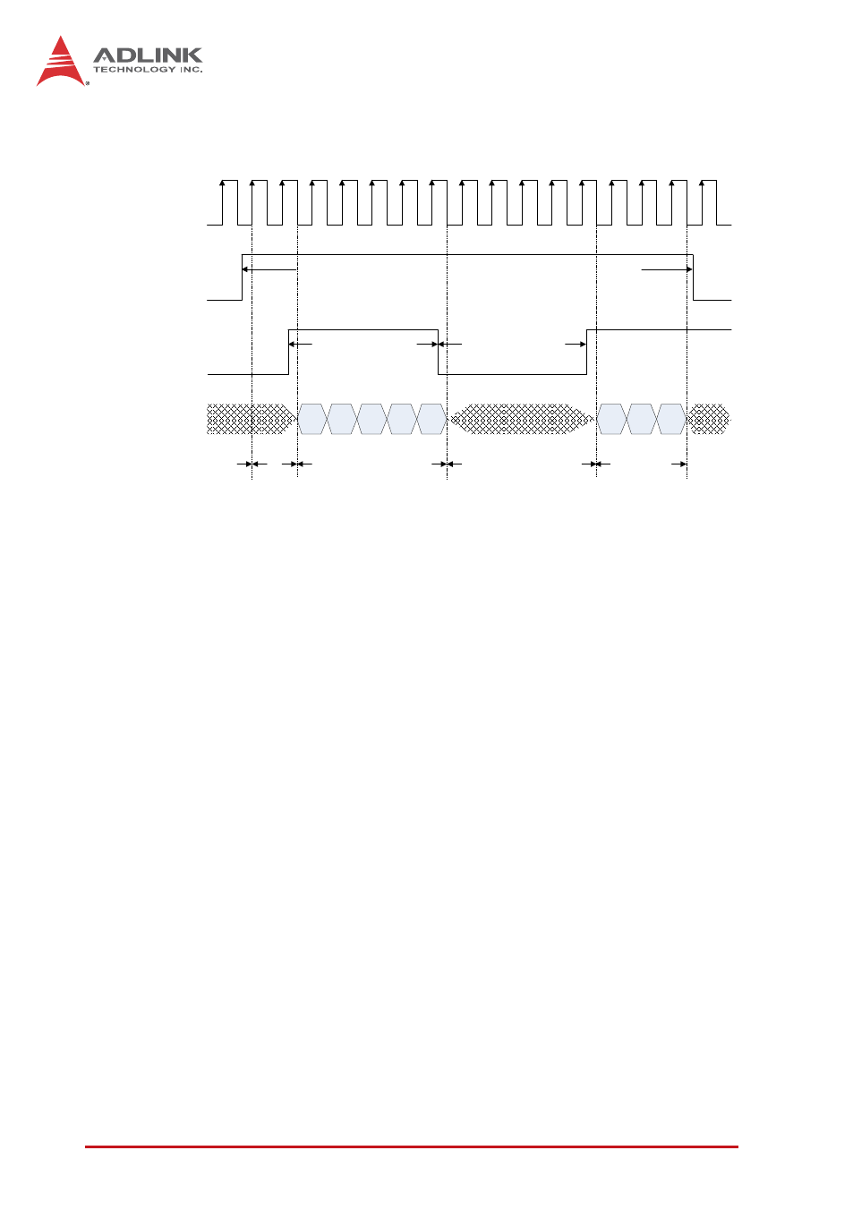
50
Operations
Timing of DI DMA in burst handshake mode is as shown.
Figure 3-19: DI Burst Handshake Timing Diagram
DO DMA in Burst Handshake Mode
In DO burst handshake mode, DO-REQ signal is active by
PCIe-7360 when it is ready to send out DO data. And then
DO-ACK signal should be generated by external device when it is
ready to receive DO data. Once DO-ACK is active, external device
has to keep DO-ACK active until its input buffer is almost full. The
operation sequences are listed as follows:
Step1: Configuration
X
Define DO port configuration (32/24/16/8-bits data width)
X
Define DO logic level configuration (3.3/2.5/1.8 V)
X
Define DO sample clock configuration (internal/external)
Z
If choose internal sampled clock, you can define sam-
pling clock rate to be 100 MHz/n (n = 1 to 65535)
Z
If choose external sampled clock, the phase shift func-
tion is available when external clock rate is from 20 to
100 MHz.
X
Define DO exporting sample clock configuration (AFI6/SMB
CLK out)
DO
DI Data
DI Sampled Clock
(from external)
DI -REQ
(Active High)
DI -ACK
(Active High)
D1
D2
D3
D9
D7
D8
PCIe-7360 is ready to
receive DI data
External Device is ready to send DI data
DI data transfer starts
D5
PCIe-7360 is not ready
to receive DI data
Wait DI-REQ
asserted
Wait DI-ACK
asserted
DI data transfer stops
DI data transfer re-start
(DI FIFO is full)
(DI-REQ & DI-ACK
are all asserted)
(DI-ACK is de-asserted)
(DI-REQ & DI-ACK
are all asserted)