List of figures, Figure 1-1: acquisition timing diagram – ADLINK PCIe-7360 User Manual
Page 17
Introduction
7
PCIe-7360
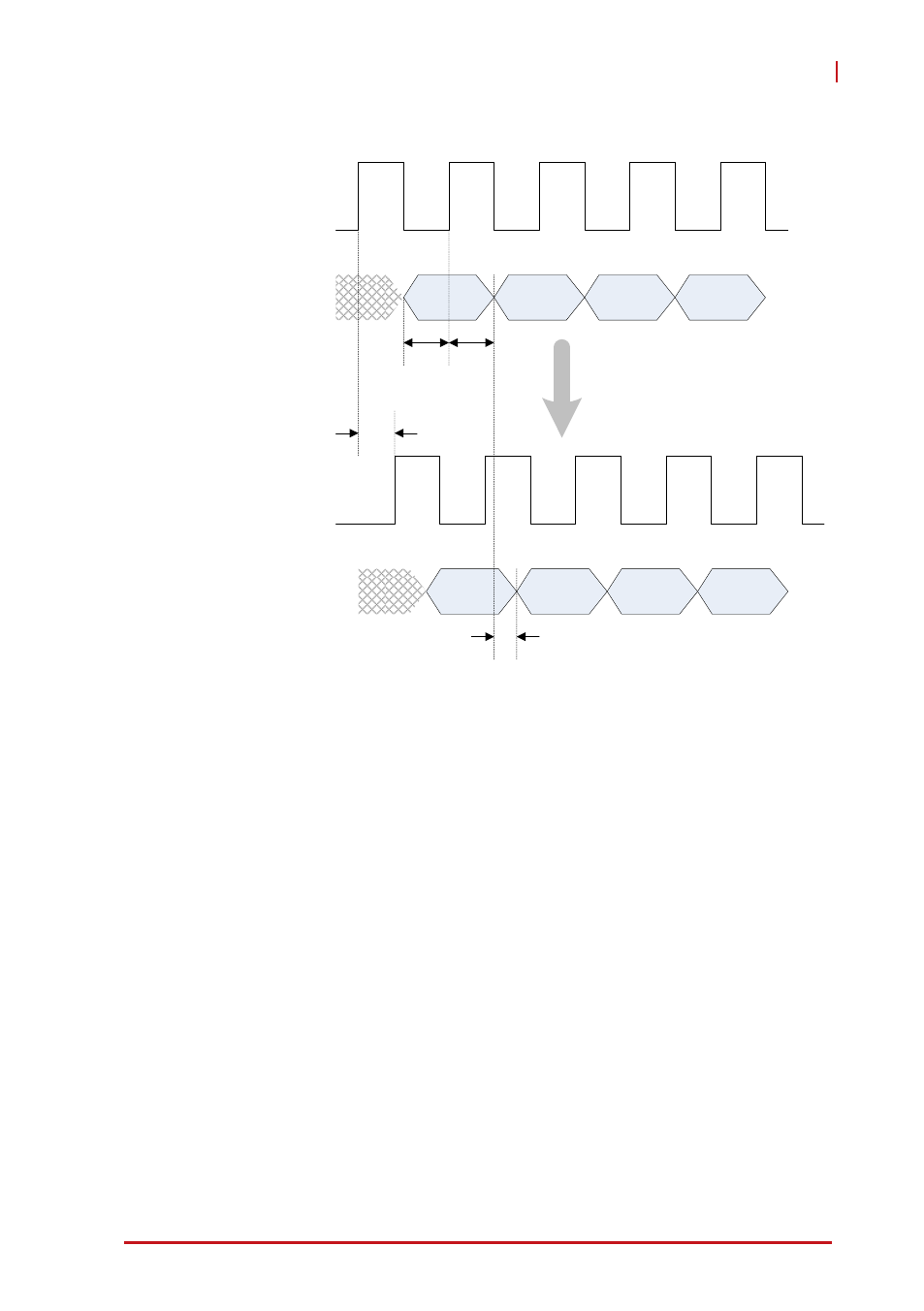
Figure 1-1: Acquisition Timing Diagram
DI Sampled Clock
(AFI7)
t
AF7D
= Time delay of external sampled clock from AFI7 to internal
t
DID
= Time delay of DI data from VHDCI connector to internal
D0
D1
D2
D3
t
AF7D
Trace & component delay
D0
D1
D2
D3
t
DID
DI Data
(connector)
DI Sampled Clock
(into FPGA)
DI Data
(into FPGA)
t
SU
t
H
See also other documents in the category ADLINK Hardware:
- USB-1901 (84 pages)
- USB-1210 (54 pages)
- USB-2401 (60 pages)
- USB-7230 (50 pages)
- USB-2405 (56 pages)
- DAQe-2010 (92 pages)
- DAQe-2204 (100 pages)
- DAQe-2213 (94 pages)
- DAQe-2501 (74 pages)
- PXI-2010 (84 pages)
- PXI-2020 (60 pages)
- PXI-2501 (62 pages)
- cPCI-9116 (98 pages)
- ACL-8112 Series (93 pages)
- ACL-8112 Series (94 pages)
- ACL-8112 Series (92 pages)
- ACL-8216 (75 pages)
- ACL-8111 (61 pages)
- PCM-9112+ (94 pages)
- PCM-9112+ (10 pages)
- cPCI-6216V (47 pages)
- ACL-6126 (28 pages)
- ACL-6128A (40 pages)
- PCM-6308V+ (52 pages)
- PCM-6308V+ (4 pages)
- PCI-7444 (82 pages)
- PCI-7434 (48 pages)
- PCI-7234 (56 pages)
- PCI-7260 (66 pages)
- PCI-7258 (38 pages)
- PCI-7256 (48 pages)
- PCI-7250 (48 pages)
- LPCI-7250 (48 pages)
- PCI-7396 (65 pages)
- PCI-7296 (59 pages)
- PCI-8554 (67 pages)
- PCIe-7350 (86 pages)
- PCIe-7300A (114 pages)
- PCIe-7200 (51 pages)
- PCI-7300A (112 pages)
- PCI-7300A (83 pages)
- PCI-7200 (96 pages)
- cPCI-7300 (83 pages)
- cPCI-7300 (82 pages)