2 programmable logic level, Programmable logic level, Figure 3-1: pcie-7360 block diagram – ADLINK PCIe-7360 User Manual
Page 32: 22 operations
22
Operations
.
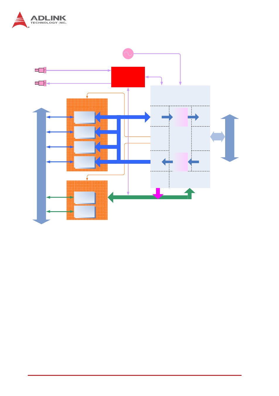
Figure 3-1: PCIe-7360 Block Diagram
3.2 Programmable Logic Level
To interface different logic level applications, the PCIe-7360 sup-
ports three software selectable logic levels of 1.8 V, 2.5 V, or 3.3 V
(5 V compatible) for all digital I/O lines, sample clocks, I
2
C, SPI,
triggers, and events. All I/O lines conform to the selected logic
Level Shifter
VH
DC
I-6
8P
C
O
N
N
E
C
T
O
R
I
N
T
ER
FA
CE
P
C
I Ex
pr
ess
x
4
IN
TE
RF
AC
E
AFI
Interface
ADLINK
Smart
Control
Engine
I2C/SPI
Pattern
Acquisition/ Generation
Timing Control
PC
Ie
IN
TE
RF
AC
E
E
x
t.
C
L
K
in/
out
DI La
tch
DO
Bu
ffe
r
DI DMA
DO
D
M
A
L
ogi
c L
e
v
e
l
Con
tro
l
Ext. CLK out
Ext. CLK in
8K FIFO
20K
FIFO
DIO[7..0]
1.8/2.5/3.3V
Logic Level Selectable
DIO[15..8]
DIO[23..16]
DIO[31..24]
AFI[5..0]
DO DATA
DI DATA
80-Step Phase
Shift Control
100MHz OSC
SMB IN
SMB OUT
Level Shifter
Level Shifter
Level Shifter
Level Shifter
1.8/2.5/3.3V
Logic Level Selectable
AFI BUS
Int. Timebase
Level Shifter
AFI[7,6]