Figure 3-6: phase shift of sample clock, 28 operations – ADLINK PCIe-7360 User Manual
Page 38
28
Operations
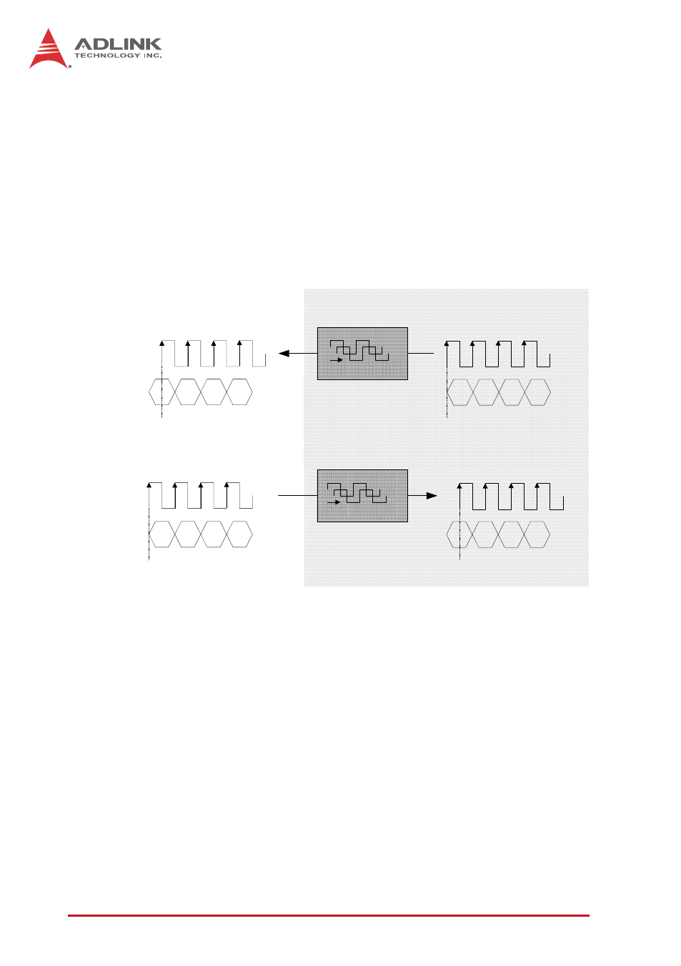
other words, the phase shift of sample clock is 4.5° x N, where N is
any integer from 1 to 80. Furthermore, in phase shifting mode, the
supported clock frequency is from 20 to 100 MHz. This function
can optimize the timing of digital pattern acquisition or generation
to avoid sampling/exporting the data from/to DUT at transition
state. Therefore, for digital input, the data can be sampled in clean
and valid timing instead of transition timing. For digital output, it
can fine tune the exporting clock to avoid the sampling of DUT at
setup time or hold time instead of aligning the data.
Figure 3-6: Phase Shift of Sample Clock
Acquisition of Digital Data
External
sampled clock
(from DUT)
DI Data
(from DUT)
Generation of Digital Data
Exported
sampled clock
(to DUT)
DO Data
(to DUT)
D0
D1
D2
D3
D0
D1
D2
D3
D0
D1
D2
D3
D0
D1
D2
D3
80-step phase shift
PCIe-7360 Card
Valid area
Transition area
Valid area
Transition area
x
80-step phase shift