6 external clock i/o specification, 7 i2c master specification, 6 external clock i/o specification 1.3.7 i – ADLINK PCIe-7360 User Manual
Page 19: C master specification
Introduction
9
PCIe-7360
1.3.6
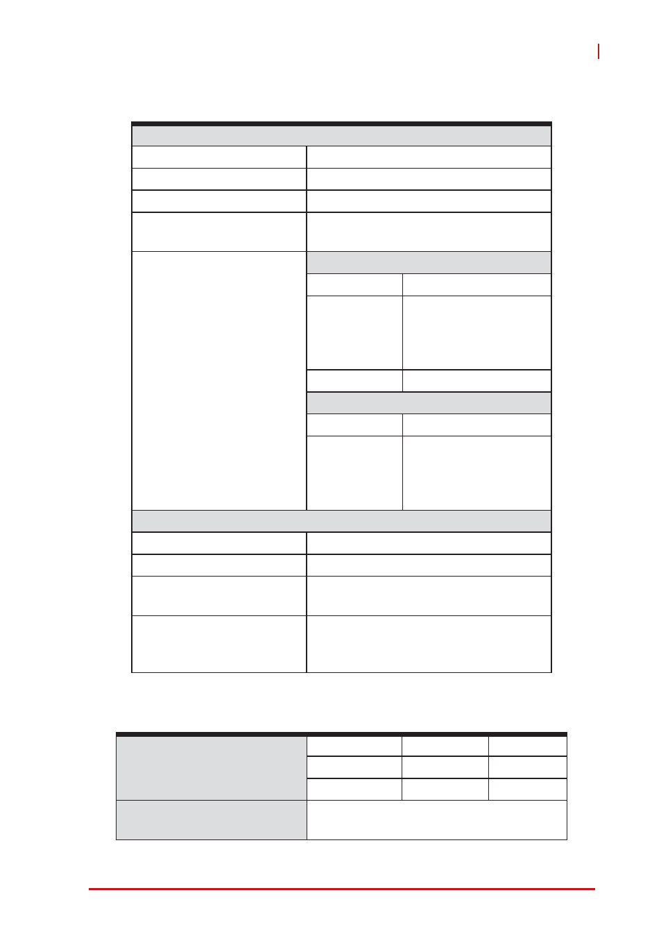
External Clock I/O Specification
1.3.7
I
2
C Master Specification
CLK IN (SMB Jack Connector)
Destination
DI or DO sample clock
Input coupling
AC
Input Impedance
50 Ω
Minimum detectable pulse
width
8 ns
External sampled clock
range
Square Wave
Voltage
0.2 Vpp to 5 Vpp
Frequency
Phase shift disabled:
0-200 MHz
Phase shift enabled:
20MHz - 100MHz
Duty cycle
40% - 60%
Sine Wave
Voltage
0.2 Vpp to 5 Vpp
Frequency
Phase shift disabled:
0-200 MHz
Phase shift enabled:
20MHz - 100MHz
CLK OUT (SMB Jack Connector)
Sources
DI or DO internal sample clock
Source impedance
50 Ω
Logic Levels
(programmable)
The same logic level of AFI I/O (1.8 V,
2.5 V, or 3.3 V)
Driving Capacity (Max.)
±8 mA at 1.8 V
±16 mA at 2.5 V
±32 mA at 3.3 V
Signal
Direction
Pin
SCL
O
AFI0
SDA
I/O
AFI1
Supported clock rate
(programmable)
1.9 kHz -244.14 kHz;
488.28125 kHz / (n + 1); 1 ≤ n ≤ 255