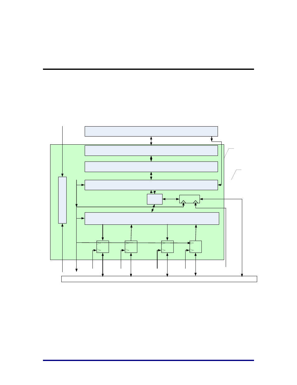
Design overview, Figure 1: pcie with dma block diagram, Figure 1 – Achronix Speedster22i PCIe User Manual
Page 8: Figure 2
UG030, April 26, 2013
8
Design Overview
The PCI Express (PCIe) standard can be implemented in the Achronix22i device.
a block diagram of the PCIe hard IP with the DMA core for high-speed data transfer to/from the
user fabric.
shows the DMA’s major interfaces, which will be discussed later.
DMA BE core
S2C
C2S
ATar
AMas
S2c_aclk[1:0]
C2S_aclk[1:0]
m_aclk
t_aclk
Transaction Layer
Bypass_clk
VC_interface
Link Layer
PHY Layer
Serdes 8 lanes (PMA)
Data/control for Fabric
Clk ( serdes 0
– pll word clk )
DMA Bypass
interface
PCIe core with DMA
C
o
n
fi
g
/
re
g
is
te
rs
Apb_pclk
CLK
i_po_ctl_clk(FCU)
PCIe- IP Clocks
MUX
Figure 1: PCIe with DMA Block Diagram