Figure 4: timing diagram for target interface, Figure 4 – Achronix Speedster22i PCIe User Manual
Page 12
UG030, April 26, 2013
12
0
31ff 8000
2
4
0
0
0000 0000 0000 0000 0000 0000 0000 0000
t_areset_n
St1
t_aclk
St1
t_awvalid
St0
St1
t_awready
3'h0
t_awregion[2:0]
t_awaddr[31:0]
4'h0
t_awlen[3:0]
3'h4
t_awsize[2:0]
St0
t_wvalid
St0
t_wready
t_wdata[127:0]
t_wstrb[15:0]
St1
t_wlast
St0
t_bvalid
St1
t_bready
2'h0
t_bresp[1:0]
St0
t_arvalid
St0
t_arready
3'h0
t_arregion[2:0]
t_araddr[31:0]
4'h0
t_arlen[3:0]
3'h4
t_arsize[2:0]
St0
t_rvalid
St1
t_rready
t_rdata[127:0]
2'h0
t_rresp[1:0]
St1
t_rlast
0
000 0000 0000 0000 0000
31ff 8080
*0
...
...
...
...
...
...
...
...
...
...
...
...
...
...
...
...
...
...
...
...
...
...
...
...
...
...
...
000f
f000
* 0002 0000 0000
* 8080
31ff 8084
31ff 8088
31ff 808c
* aea1 0001 0000
00 0000 0000
0
0
0
4
0
4
0
0
4
0
00f0
0007 0006 0000 0000 0000 1a2ab733
0000
0000 0000 0000
...
...
...
...
...
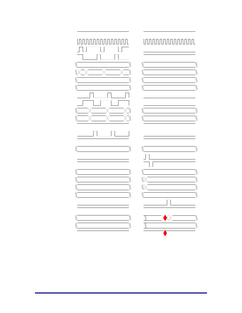
Figure 4: Timing Diagram for Target Interface
Moreover, the AXI Target Interface implements FIFOs to buffer multiple
writes and reads simultaneously to enable maximum bandwidth.
The AXI Target Interface implements a dual clock interface. The AXI clock
domain may be different than the PCI Express clock domain. Gray Code