Figure 6, The system-to-card dma interface – Achronix Speedster22i PCIe User Manual
Page 14
UG030, April 26, 2013
14
transactions for this packet. This allows the user hardware design to
implement FIFOs for some AXI DMA transactions while simultaneously also
supporting addressable RAM for other AXI DMA transactions.
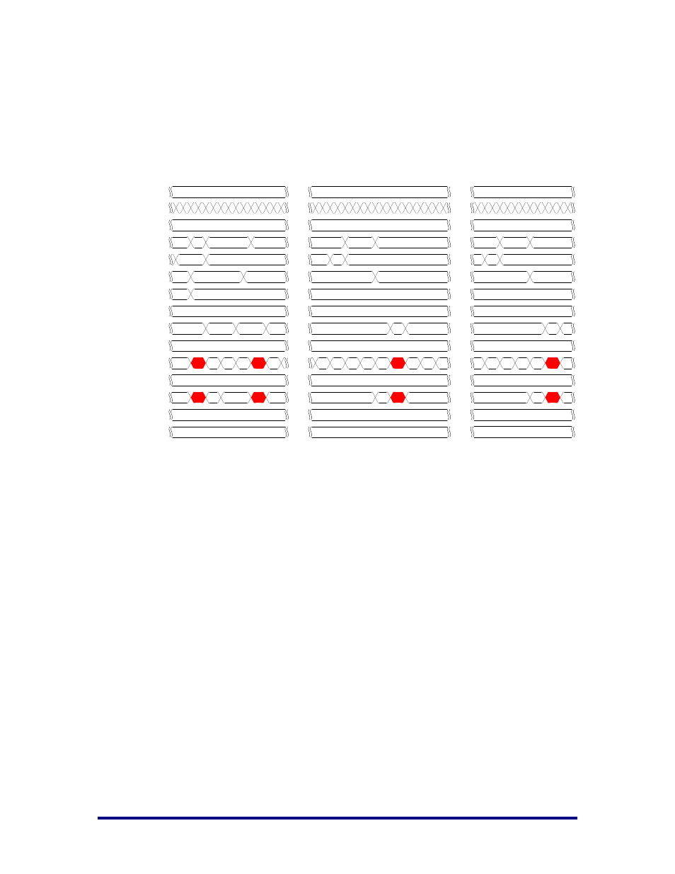
depicts the Card-to-System DMA interface and
the System-to-Card DMA interface.
c2s_areset_n[1:0]
2'h3
c2s_aclk[1:0]
2'h0
c2s_fifo_addr_n[1:0]
2'h3
c2s_arvalid[1:0]
2'h0
c2s_arready[1:0]
2'h3
c2s_araddr[71:0]
c2s_arlen[7:0]
8'h00
c2s_arsize[5:0]
6'h24
c2s_rvalid[1:0]
2'h0
c2s_rready[1:0]
2'h3
c2s_rdata[255:0]
c2s_rresp[3:0]
4'h0
c2s_rlast[1:0]
2'h0
c2s_ruserafull[1:0]
2'h0
c2s_ruserstrb[31:0]
3
0
*3
*3
*3
*3
*3
0
000 b000 0000
2
0
0
2
0
0
2
2
0
f5
0
3
*3
*3
*3
*3
*3
*3
*f3
*3
3
0
0000 0000
0
3
*4
*5
*3
*3
2
0
* 0000 2400
2
0
2
0
2
...
...
...
...
...
...
...
...
...
...
...
...
...
...
...
...
...
...
...
...
...
...
...
...
...
...
...
...
...
...
3
3
3
0
2
0
00 0000 9000 0000 2400
00 0000 a000 0000 2400
15
f5
24
24
f5
24
0
0
2
2
2
2
2
0
0
0
3
3
0
0
0
0
0
0
0
0000 0000
0000 0000
0
2
0
00 0000 a000 0000 2400
00 0000 9000 0000
2400
6665
*3
...
...
...
Figure 5: Timing Diagram for Card-to-System DMA Interface