Sdmc register map, Sdram_mode register – Rainbow Electronics AT75C220 User Manual
Page 27

AT75C220
27
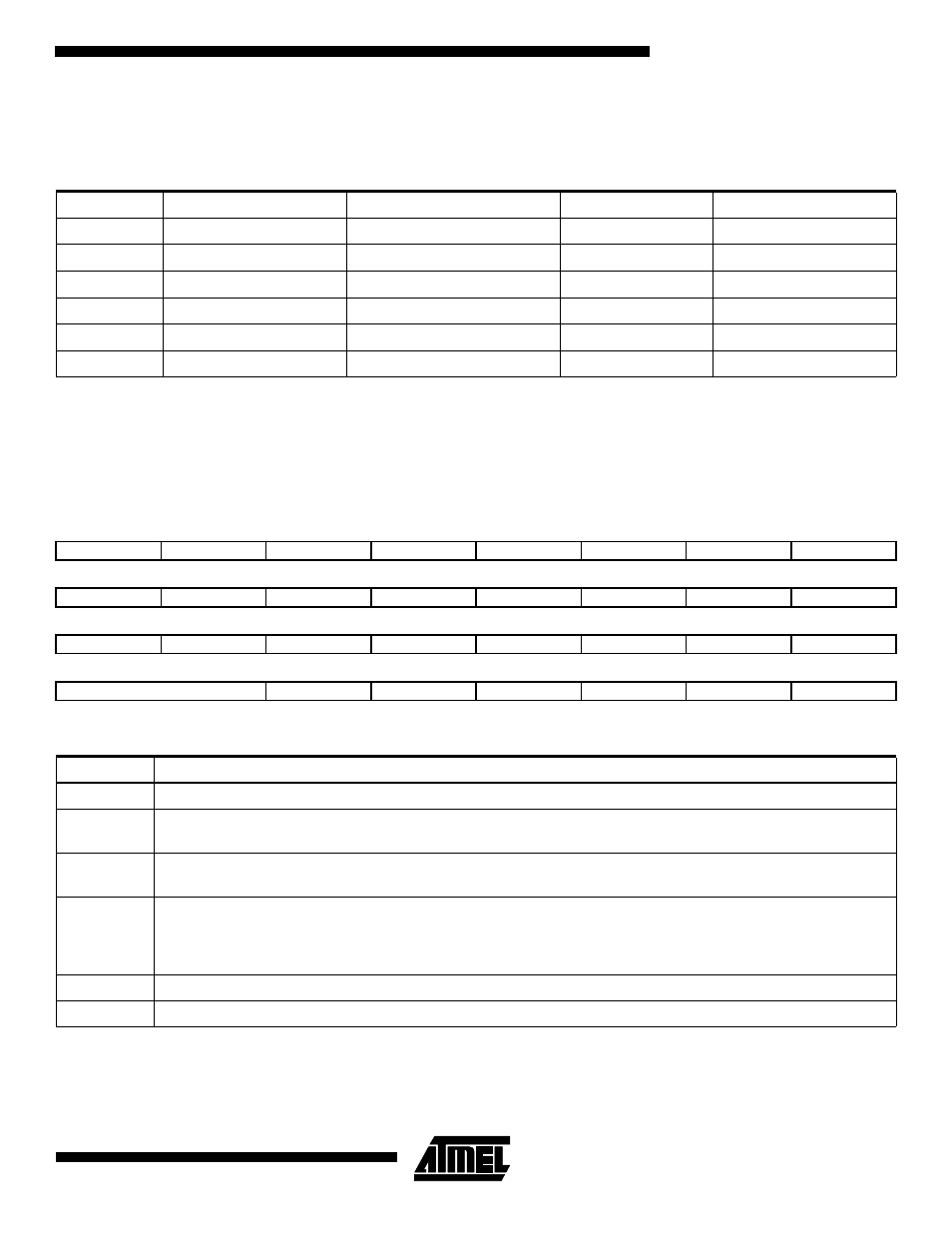
SDMC Register Map
Base Address: 0xFF008000
SDRAM_MODE Register
Register Name: SDRAM_MODE
Access Type: Read/write
Reset Value: 0x0
•
MODE
Table 12. SDMC Register Map
Offset
Register Name
Description
Access
Reset Value
0x0000
SDRAM_MODE
Mode Register
Read/write
0x00000000
0x0004
SDRAM_TIMER
Timer Register
Read/write
0x00000000
0x0008
SDRAM_CFG
Configuration Register
Read/write
0x00000000
0x000C
SDRAM_16BIT
Selects 16-/32-bit modes
Read/write
0x00000001
0x0010
SDRAM_CS0_ADDR
Base address for CS0
Read/write
0x00000040
0x0014
SDRAM_CS1_ADDR
Base address for CS1
Read/write
0x00000050
31
30
29
28
27
26
25
24
–
–
–
–
–
–
–
–
23
22
21
20
19
18
17
16
–
–
–
–
–
–
–
–
15
14
13
12
11
10
9
8
–
–
–
–
–
–
–
MODE
7
6
5
4
3
2
1
0
MODE
–
–
–
–
–
–
MODE
Description
000
Normal mode. Any access to the SDRAM will be decoded normally.
001
The NOP command is issued to the SDRAM when the host accesses the SDRAM memory area, regardless of the
cycle.
010
The all banks precharge command is issued to the SDRAM when the host accesses the SDRAM memory area,
regardless of the cycle.
011
The load mode register command is issued to the SDRAM when the host accesses the SDRAM memory area,
regardless of the cycle. The address offset with respect to the SDRAM memory base address is used to program the
mode register. For example, when this mode is activated, an access to the “SDRAM_BASE + offset” generates a load
mode register command with the value offset written to the mode register of the SDRAM.
100
A refresh command is issued to the SDRAM. An all banks precharge command must precede.
others
Reserved
