Ds1862 xfp laser control and digital diagnostic ic – Rainbow Electronics DS1862 User Manual
Page 37
DS1862
XFP Laser Control and Digital Diagnostic IC
____________________________________________________________________
37
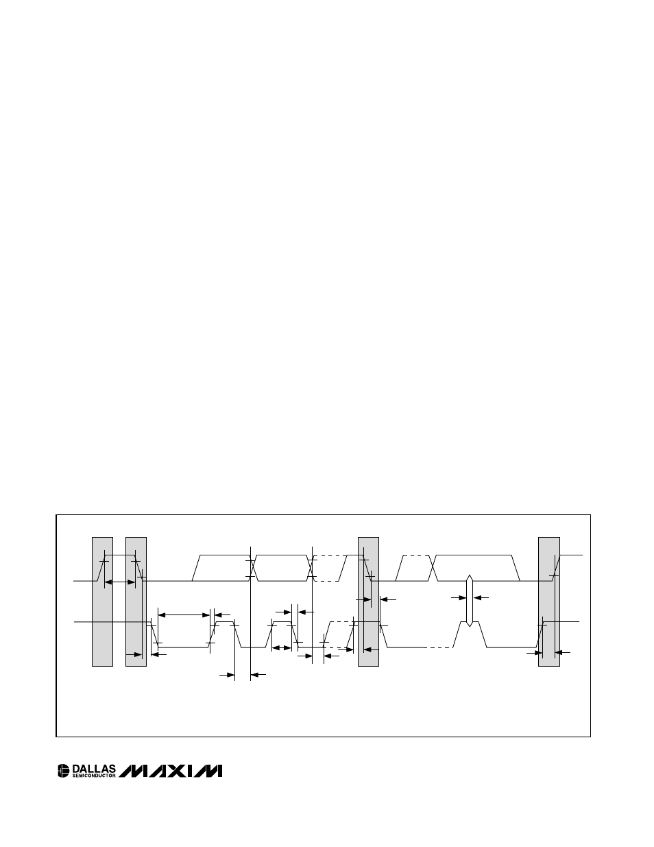
Bit write: Transitions of SDA must occur during the low
state of SCL. The data on SDA must remain valid and
unchanged during the entire high pulse of SCL plus the
setup and hold time requirements (Figure 14). Data is
shifted into the device during the rising edge of the SCL.
Bit read: At the end of a write operation, the master
must release the SDA bus line for the proper amount of
setup time (Figure 14) before the next rising edge of
SCL during a bit read. The device shifts out each bit of
data on SDA at the falling edge of the previous SCL
pulse and the data bit is valid at the rising edge of the
current SCL pulse. Remember that the master gener-
ates all SCL clock pulses including when it is reading
bits from the slave.
Acknowledgement (ACK and NACK): An Acknowl-
edgement (ACK) or Not Acknowledge (NACK) is always
the 9th bit transmitted during a byte transfer. The device
receiving data (the master during a read or the slave dur-
ing a write operation) performs an ACK by transmitting a
zero during the 9th bit. A device performs a NACK by
transmitting a one during the 9th bit. Timing (Figure 14)
for the ACK and NACK is identical to all other bit writes.
An ACK is the acknowledgment that the device is prop-
erly receiving data. A NACK is used to terminate a read
sequence or as an indication that the device is not
receiving data.
Byte write: A byte write consists of 8 bits of information
transferred from the master to the slave (most signifi-
cant bit first) plus a 1-bit acknowledgement from the
slave to the master. The 8 bits transmitted by the mas-
ter are done according to the bit write definition and the
acknowledgement is read using the bit read definition.
Byte read: A byte read is an 8-bit information transfer
from the slave to the master plus a 1-bit ACK or NACK
from the master to the slave. The 8 bits of information
that are transferred (most significant bit first) from the
slave to the master are read by the master using the bit
read definition, and the master transmits an ACK using
the bit write definition to receive additional data bytes.
The master must NACK the last byte read to terminate
communication so the slave returns control of SDA to
the master.
Slave address byte: Each slave on the I
2
C bus
responds to a slave addressing byte sent immediately
following a start condition. The slave address byte con-
tains the slave address in the most significant 7 bits
and the R/
W bit in the least significant bit.
The DS1862’s slave address is 1010000Xb. The MOD-
DESEL pin is used as a chip select, and allows the
device to respond or ignore I
2
C communication that
has A0h as the device address. By writing the correct
slave address with R/
W = 0, the master indicates it will
write data to the slave. If R/
W = 1, the master will read
data from the slave. If an incorrect slave address is
written, the DS1862 assumes the master is communi-
cating with another I
2
C device and ignores the commu-
nications until the next start condition is sent.
Memory address: During an I
2
C write operation, the
master must transmit a memory address to identify the
memory location where the slave is to store the data.
SDA
SCL
t
HD:STA
t
LOW
t
HIGH
t
R
t
F
t
BUF
t
HD:DAT
t
SU:DAT
REPEATED
START
t
SU:STA
t
HD:STA
t
SU:STO
t
SP
STOP
START
NOTE: TIMING IS REFERENCED TO V
IL(MAX)
AND V
IH(MIN)
.
Figure 14. I
2
C Timing Diagram