Ds1862 xfp laser control and digital diagnostic ic, Table 8. temperature conversion examples, Table 9. internal calibration capabilities – Rainbow Electronics DS1862 User Manual
Page 19
DS1862
XFP Laser Control and Digital Diagnostic IC
____________________________________________________________________
19
Internal Calibration
The DS1862 has two means for scaling an analog input
to a digital result. The two devices alter the gain and
offset of the signal to be calibrated. All of the inputs
except internal temperature have unique registers for
both the gain and the offset that can be found in Table
04h. See the table below for a complete description of
internal calibration capabilities including right-shifting
for all monitor channels.
To scale a specific input’s gain and offset, the relation-
ship between the analog input and the expected digital
result must be known. The input that would produce a
corresponding digital result of all zeroes is the null
value (normally this input is GND). The input that would
produce a corresponding digital result of all ones is the
full-scale (FS) value minus one LSB. The FS value is
also found by multiplying an all ones digital value by
the weighted LSB. For example, a digital reading is 16
bits long, assume that the LSB is known to be 50µV,
then the FS value would be 2
16
x 50µV = 3.2768V.
A binary search can be used to find the appropriate
gain value to achieve the desired FS of the converter.
Once the gain value is determined, then it can be
loaded into the appropriate channels’ Gain register.
This requires forcing two known voltages on to the
monitor input pin. For best results, one of the forced
voltages should be the NULL input and the other
should be 90% of FS. Since the LSB of the least signifi-
cant bit in the digital reading register is known, the
expected digital results are also known for both the null
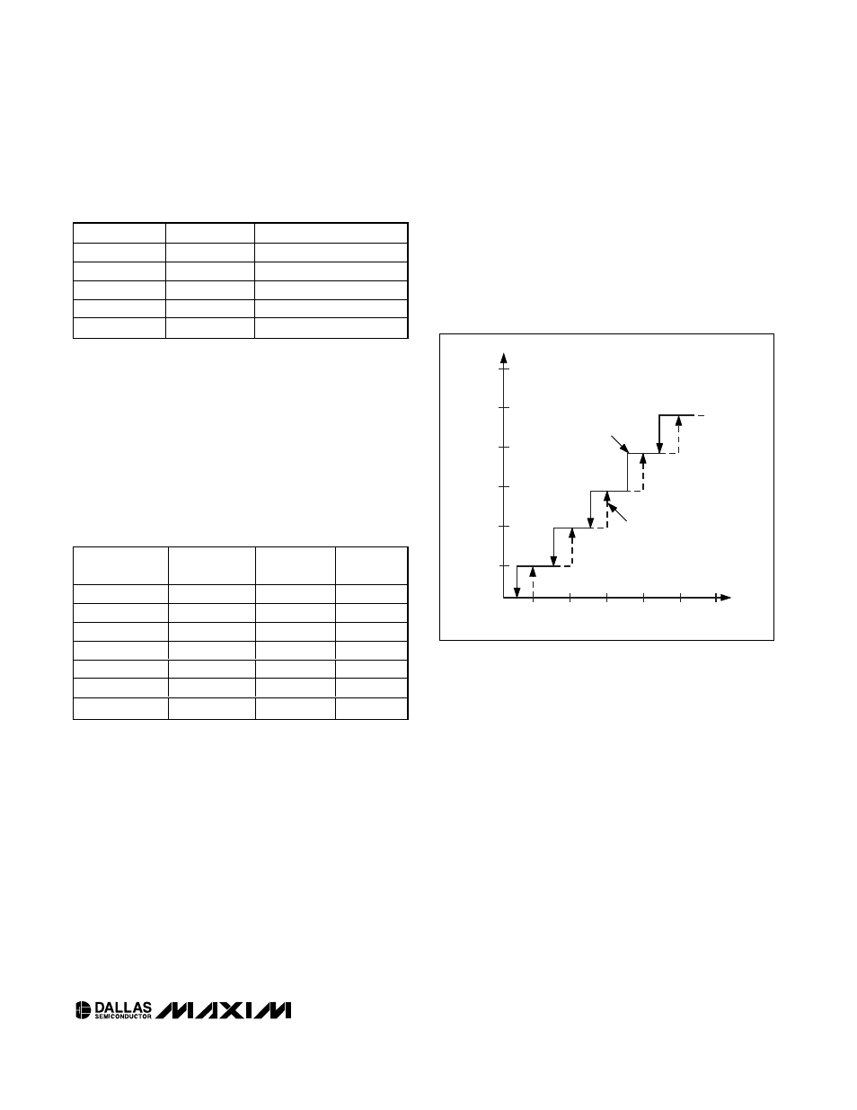
and FS value inputs. Figure 9 describes the hysteresis
built into the DS1862’s LUT functionality.
With the exception of BMD, which can source or sink
current, all monitored channels are high impedance
and are only capable of directly measuring a voltage. If
other measured quantities are desired, such as: light,
frequency, power, current etc., they must be converted
to a voltage. In this situation the user is not interested in
voltage measurement on the monitored channel, but
the measurement of the desired parameter. Only the
relationship between the indirect measured quantity
(light, frequency, power, current, etc.) to the expected
digital result must be known.
An example of gain scaling using the recommended
binary search procedure is provided with the following
pseudo-code.
To help will the computation, two integers need to be
defined: count 1 and count 2. CNT1 = NULL / LSB and
CNT2 = 90%FS / LSB. CLAMP is the largest result that
can be accommodated.
Table 8. Temperature Conversion
Examples
MSB (BIN)
LSB (BIN)
TEMPERATURE (°C)
01000000
00000000
+64
01000000
00001000
+64.03215
01011111
00000000
+95
11110110
00000000
-10
11011000
00000000
-40
Table 9. Internal Calibration Capabilities
SIGNAL
INTERNAL
SCALING
INTERNAL
OFFSET
RIGHT-
SHIFTING
Temperature
—
x
—
V
CC2/3
x
x
—
IBIASMON
x
x
x
RSSI (RX-P)
x
x
x
AUX1MON
x
x
x
AUX2MON
x
x
x
BMD (TX-P)
x
x
x
M6
M5
M4
M3
M2
M1
2
4
6
8
10
12
TEMPERATURE (
°C)
MEMORY LOCATION
INCREASING
TEMPERATURE
DECREASING
TEMPERATURE
Figure 9. Look-Up Table Hysteresis