Ds1862 xfp laser control and digital diagnostic ic – Rainbow Electronics DS1862 User Manual
Page 2
DS1862
XFP Laser Control and Digital Diagnostic IC
2
_____________________________________________________________________
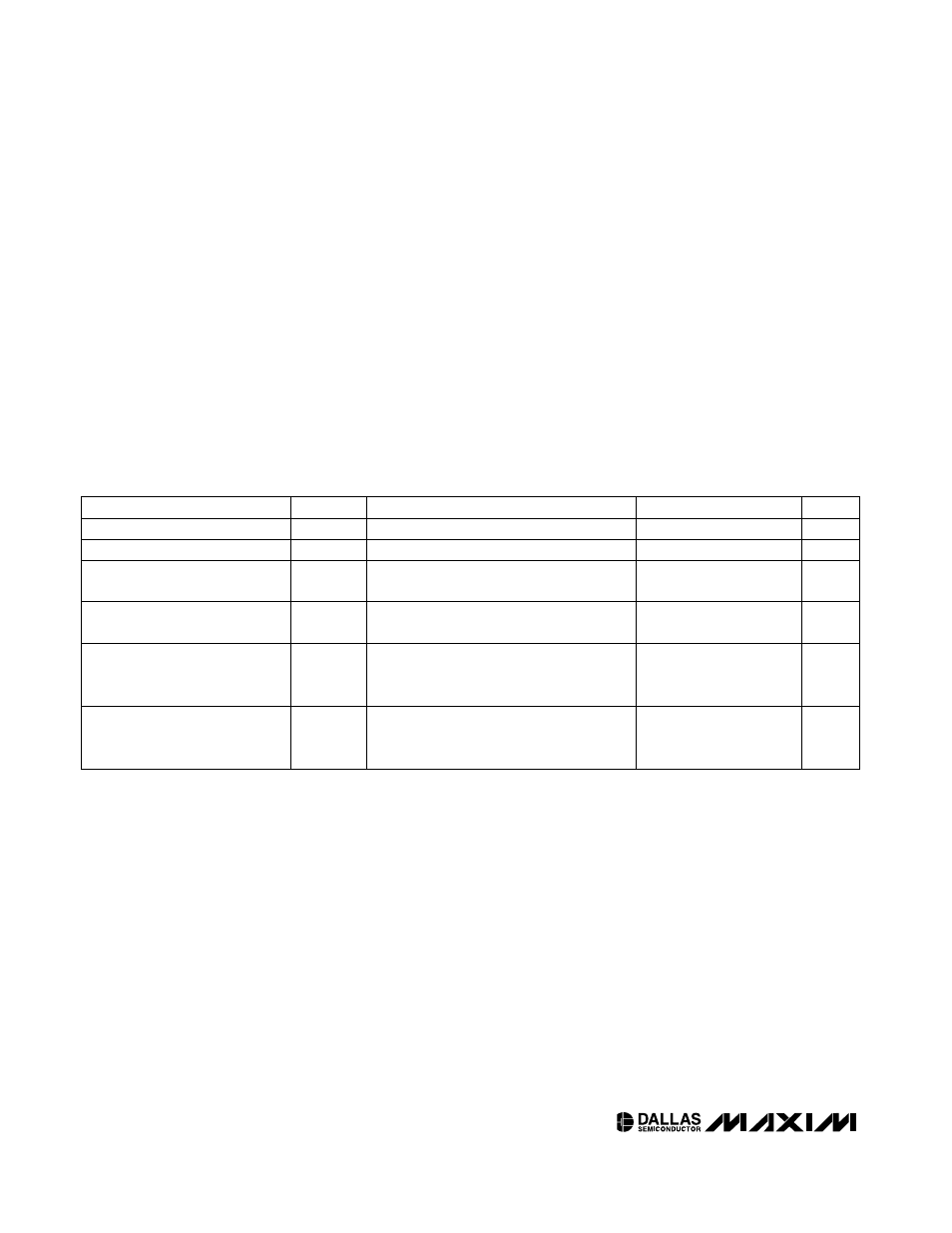
ABSOLUTE MAXIMUM RATINGS
RECOMMENDED OPERATING CONDITIONS
(V
CC3
= +2.9V to +5.5V, T
A
= -40°C to +100°C, unless otherwise noted.)
Stresses beyond those listed under “Absolute Maximum Ratings” may cause permanent damage to the device. These are stress ratings only, and functional
operation of the device at these or any other conditions beyond those indicated in the operational sections of the specifications is not implied. Exposure to
absolute maximum rating conditions for extended periods may affect device reliability.
Voltage on Any Open-Drain Pin
Relative to Ground.............................................-0.5V to +6.0V
Voltage on MOD-DSEL, SDA, SCL, FETG, THRSET, TX-D,
AUX1MON, AUX2MON, IBIASMON,
RSSI, BIASSET, MODSET, EN1,
and EN2 ............-0.5V to (VCC3 + 0.5V), not to exceed +6.0V
Voltage on SC-RX-LOS, SC-RX-LOL, RX-LOS, SC-TX-LOS,
MOD-NR, EN1,
and EN2 ............-0.5V to (VCC2 + 0.5V), not to exceed +6.0V
Operating Temperature Range .........................-40°C to +100°C
EEPROM Programming Temperature Range .........0°C to +70°C
Storage Temperature Range .............................-55°C to +125°C
Soldering Temperature...................See J-STD-020 Specification
PARAMETER
SYMBOL
CONDITIONS
MIN
TYP
MAX
UNITS
Main Supply Voltage
V
CC3
(Note 1)
+2.9
+5.5
V
Secondary Supply Voltage
V
CC2
V
CC2
not to exceed V
CC3
(Note 2)
+1.6
+3.6
V
High-Level Input Voltage
(SDA, SCL)
V
IH
I
IH
(max) = 10µA
0.7 x
V
CC3
V
CC3
+
0.5
V
Low-Level Input Voltage
(SDA, SCL)
V
IL
I
IL
(max) = -10µA
GND -
0.3
0.3 x
V
CC3
V
High-Level Input Voltage
(TX-D, MOD-DESEL,
P-DOWN/RST) (Note 3)
V
IH
I
IH
(max) = 10µA
2
V
CC3
+
0.3
V
Low-Level Input Voltage
(TX-D, MOD-DESEL,
P-DOWN/RST) (Note 3)
V
IL
I
IL
(max) = -10µA
-0.3
+0.8
V