Ds1862 xfp laser control and digital diagnostic ic, Table 4. monitor channel fs and lsb detail – Rainbow Electronics DS1862 User Manual
Page 17
DS1862
XFP Laser Control and Digital Diagnostic IC
____________________________________________________________________
17
Monitor Channels
The DS1862 has seven monitored voltage signals that
are polled in a round-robin multiplexed sequence and
are updated with the frame rate, t
FRAME
. All channels
are read as 16-bit values, but have 13-bit resolution,
and with the exception of temperature measurements,
all channels are stored as unsigned values. The resulting
16-bit value for all monitored channels, except internal
temperature, is calculated by internally averaging the
analog-to-digital result 8 times. The resulting internal
temperature monitor channel is averaged 16 times. See
the Internal Calibration section for a complete descrip-
tion of each channel’s method(s) of internal calibration.
The AUX1MON, AUX2MON, and V
CC2/3
monitor chan-
nels are optional and can be disabled. This feature
allows for shorter frame rate for the essential monitor
channels. Channels that can not be disabled are: inter-
nal temperature, BMD, RSSI, and IBIASMON. A table of
full-scale (FS) signal values (using factory internal cali-
bration without right shifting) and the resulting FS code
values for all seven channels is provided below.
Measuring Temperature—Internal or External
The DS1862 is capable of measuring temperature on
three different monitor channels: internal temperature
sensor, AUX1MON, and AUX2MON. Only the internal
temperature and AUX2MON channels are capable of
indexing the LUT to control the extinction ratio. To use
an external temperature sensor on AUX2MON, the
TEMP_INT/EXT bit in Table 04h, Byte 8Bh, must be set.
While AUX2MON controls the extinction ratio, the inter-
nal temperature sensor does not stop running; despite
extinction ratio control by AUX2MON, it is this internal
temperature signal that continues to control the status
of temperature flags. Also when TEMP_INT/EXT = 1, the
internal temperature clamps at -40°C and +103.9375°C,
and when TEMP_INT/EXT = 0 it clamps at -120°C and
+127.984°C. AUX2MON, however, does have its own flag
to indicate an out-of-tolerance condition and assert the
INTERRUPT pin.
Both AUX1MON and AUX2MON can be used to mea-
sure temperature as a function of voltage on their
respective pins. They can be enabled by selecting
either 0h or 4h from Table 5. Internal (or external) cali-
bration may be required to transmute the input voltage
to the desired two’s-complement digital code, readable
from the result registers in lower memory, Bytes 6Ah,
6Bh and 6Ch, 6Dh.
Measuring V
CC2/3
The DS1862 has the flexibility to internally measure
either V
CC2
or V
CC3
to monitor supply voltage. V
CC2
or
V
CC3
is user selectable by the V
CC2/3
_Sel bit in Table
01h, Byte DCh. To remove V
CC2/3
from the round-robin
monitor update scheme, despite having V
CC2
or V
CC3
selected to be monitored, the Reserve_EN bit in Table
04h, Byte 8Bh can be programmed to a 0. The analog
power-on-reset flag, POA, indicates the status of V
CC3
power supply. Even though POA seems to behave simi-
larly to V
CC2/3
monitor channel, it is completely sepa-
rate and has no connection.
Measuring APC and Laser Parameters—BMD,
IBIASMON, RSSI
BMD and BIASSET are used to control and monitor the
laser functionality. Regardless of the set BMD current in
the APC register, the DS1862 measures BMD pin cur-
rent and uses this value not only to adjust the current
on the BIASSET pin, but also to monitor TX-P as well.
The IBIASMON pin is used to input a voltage signal to
the DS1862 that can be used to monitor the bias cur-
rent through the laser. This monitor channel does not
drive the HIGHBIAS quick-trip (QT) alarms for safety
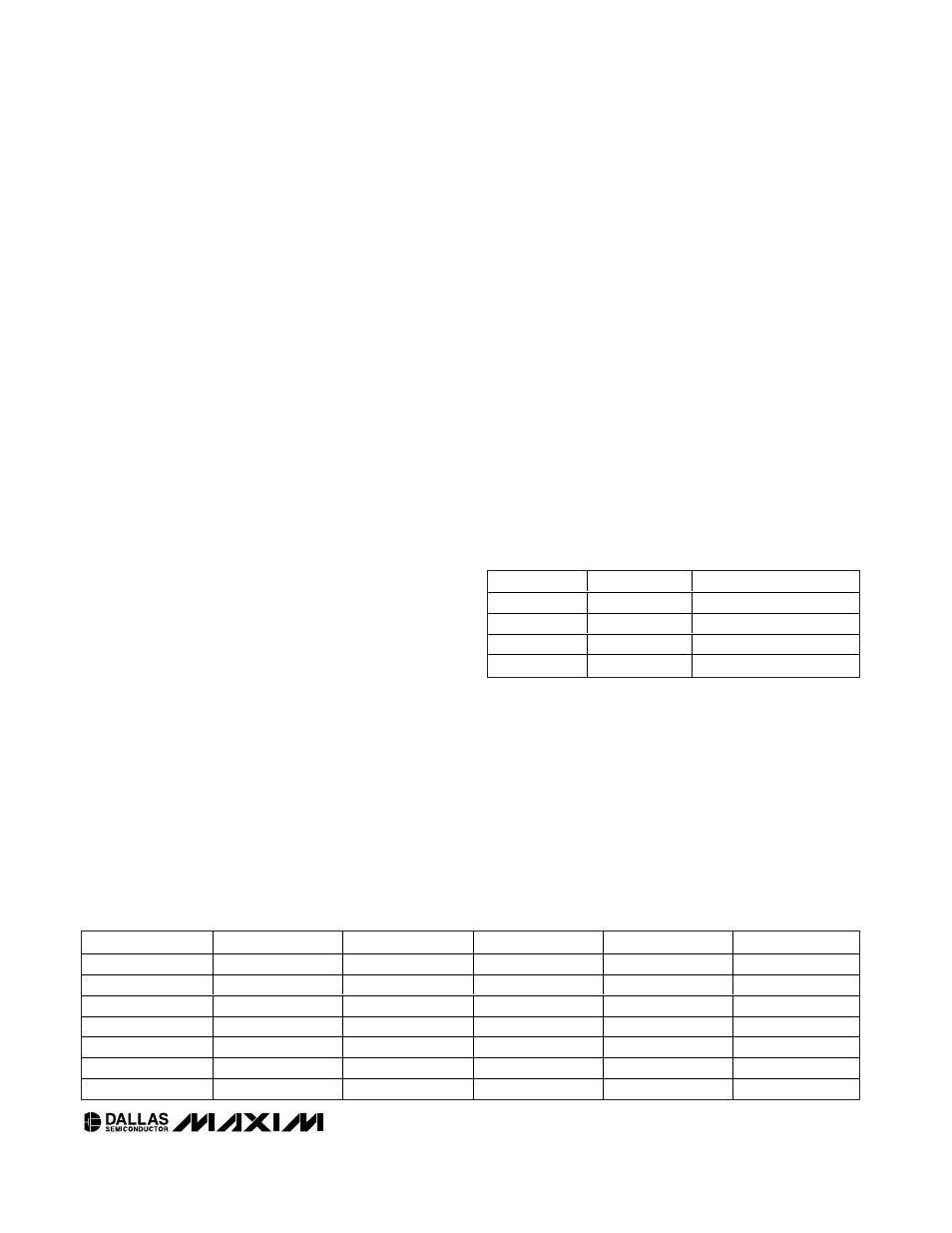
Table 4. Monitor Channel FS and LSB Detail
SIGNAL
+FS SIGNAL
+FS (hex)
-FS SIGNAL
-FS (hex)
LSB
Temperature
127.984°C
7FF8
-120°C
8800
0.0625°C
V
CC2/3
6.5528V
FFF8
0V
0000
100µV
IBIASMON
2.4997V
FFF8
0V
0000
38.147µV
RSSI
2.4997V
FFF8
0V
0000
38.147µV
AUX1MON
6.5528V
FFF8
0V
0000
38.147µV
AUX2MON
6.5528V
FFF8
0V
0000
38.147µV
BMD (TX-P)
1.5mA
FFF8
0mA
0000
22.888nA
RESERVE_EN
V
CC2/3_Sel
RESULT
0
0
V
CC2/3
result not enabled.
0
1
V
CC2/3
result not enabled.
1
0
V
CC3
is being measured.
1
1
V
CC2
is being measured.