Rf22 – Rainbow Electronics RF22 User Manual
Page 76
RF22
Version: 0.1 Date: 12/23/2008
Tel: +86-755-82973805 Fax: +86-755-82973550 E-mail: [email protected] http://www.hoperf.com
76
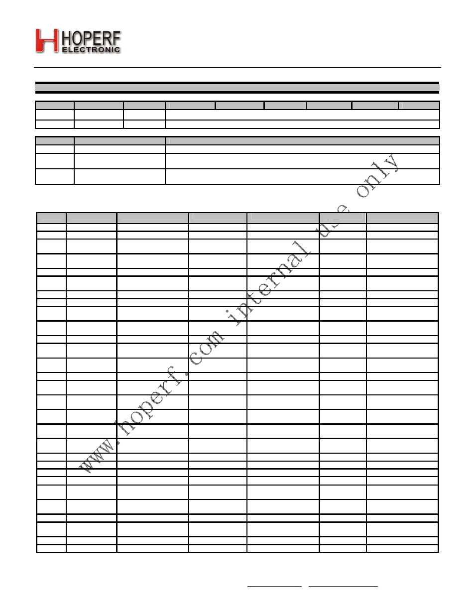
Register 51h. Digital Test Bus Select
Bit
D7
D6
D5
D4
D3
D2
D1
D0
Name
Reserved
ensctest
dtb[5:0]
Type
R/W
R/W
R/W
Reset value = 00000000
Bit
Name
Function
7
Reserved
Reserved.
6
ensctest
Scan Test Enable.
When set to 1 then GPIO0 will be the ScanEn input.
5:0
dtb[5:0]
Digital Test Bus.
GPIO must be configured to Digital Test Mux Output.
Table37. Internal Digital Signals Available on the Digital Test Bus
dtb[4:0]
GPIO0
Signal
GPIO1
Signal
GPIO2
Signal
0
wkup_clk_32k
wake-up 32kHz clock
rbase_en
first divided clock
clk_base
timebase clock
1
wkup_clk_32k
wake-up 32kHz clock
wake_up
wake-up event
tm1sec
1 sec timebase
2
ts_adc_en
aux. ADC enable
adc_rdy_n
aux. ADC conversion
ready
adc_done
aux. ADC measurement
done
3
cont_lbd
low battery continuous
mode
lbd_on
low battery ON signal
lbd
unfiltered output of LBD
4
div_clk_g
gated divided clock
uc_clk
microcontroller clock
ckout_rcsel
slow clock selected
5
en_div_sync
clock divider enable
(sync'ed)
en_ckout
clock out enable
en_ckout_s
clock out enable
(sync'ed)
6
osc30_en
oscillator enable
osc30_bias2x
oscillator bias control
xok
chip ready
7
xok
chip ready
zero_cap
cap. load zero
osc30_buff_en
buffer enable
8
tsadc_needed
aux. ADC enable
ext_retran
ext. retransmission
request
tx_mod_gpio
TX modulation input
9
gpio_0_oen_n
GPIO0 output enable
gpio_0_aen
GPIO0 analog selection
gpio_0_aden
GPIO0 ADC input line
enable
10
int_ack1
interrupt acknowledge 1
int_ack2
interrupt acknowledge 2
int_store
interrupt latch closed
11
ext_int2
ext. interrupt from
GPIO2
irq_bit8
combined external
status
msk_bit8
combined masked ext.
int.
12
sdo_aux_sel
SDO aux. function select
sdo_aux
SDO aux. signal
nirq_aux_sel
nIRQ aux. function
select
13
trdata_on_sdi
TX/RX data on SDI
tx_mod
TX modulation input
tx_clk_out
TX clock output
14
start_full_sync
RC osc. full calibration
start
start_fine_sync
RC osc. fine calibration
start
xtal_req
crystal req. for RC osc.
cal.
15
coarse_rdy
RC osc. coarse cal.
ready
fine_rdy
RC osc. fine cal. ready
xtal_req_sync
sync'ed crystal request
16
vco_cal_rst_s_n
VCO calibration reset
vco_cal
VCO calibration is
running
vco_cal_done
VCO calibration done
17
vco_cal_en
VCO calibration enable
en_ref_cnt
reference counter
enable
en_freq_cnt_s
frequency counter
enable
18
vco_cal_en
VCO calibration enable
pos_diff
positive difference to
goal
en_freq_cnt_s
frequency counter
enable
19
dsm_clk_mux
DSM multiplexed clock
pll_fb_clk_tst
PLL feedback clock
pll_ref_clk_tst
PLL reference clock
20
dsm[0]
delta-sigma output
dsm[1]
delta-sigma output
dsm[2]
delta-sigma output
21
dsm[3]
delta-sigma output
pll_fbdiv15
dsm_rst_s_n
delta-sigma reset
22
pll_en
PLL enable: TUNE state
pllt0_ok
PLL initial settling OK
pllts_ok
PLL soft settling OK
23
ch_freq_req
frequency change
request
pllts_ok
PLL soft settling OK
vco_cal_done
VCO calibration done
24
vco_cal_en
VCO calibration enable pll_vbias_shunt_en
VCO bias shunt enable
prog_req
frequency recalculation
req.
25
bandgap_en
bandgap enable
frac_div_en
fractional divider enable
buff3_en
buffer3 enable
26
pll_pfd_up
PFD up signal
pll_pfd_down
PFD down signal
pfd_up_down
PFD output change
(XOR'ed)
27
pll_lock_detect
PLL lock detect
pll_en
PLL enable: TUNE state
pllt0_ok
PLL initial settling OK
28
pll_en
PLL enable: TUNE state
pll_lock_detect
PLL lock detect
pllts_ok
PLL soft settling OK