Rf22, Definition of test conditions, Table8. absolute maximum ratings – Rainbow Electronics RF22 User Manual
Page 5
RF22
Version: 0.1 Date: 12/23/2008
Tel: +86-755-82973805 Fax: +86-755-82973550 E-mail: [email protected] http://www.hoperf.com
5
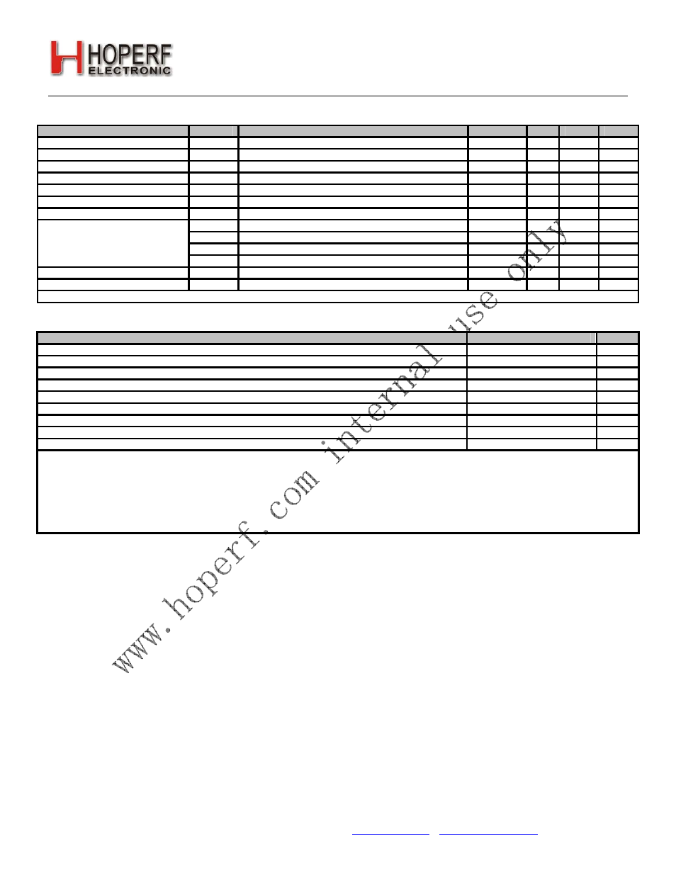
Table7. GPIO Specifications (GPIO_0, GPIO_1, and GPIO_2)
Parameter
Symbol
Conditions
Min
Typ
Max
Units
Rise Time
T
RISE
0.1 x V
DD
to 0.9 x V
DD
, C
L
= 10 pF, DRV<1:0>=HH
—
—
8
ns
Fall Time
T
FALL
0.9 x V
DD
to 0.1 x V
DD
, C
L
= 10 pF, DRV<1:0>=HH
—
—
8
ns
Input Capacitance
C
IN
—
—
1 pF
Logic High Level Input Voltage
V
IH
V
DD
– 0.6
—
V
Logic Low Level Input Voltage
V
IL
—
—
0.6
V
Input Current
I
IN
0 IN < V DD –100 — 100 nA Input Current If Pullup is Activated I INP V IL =0 V 5 — 25 μA I OmaxLL DRV<1:0>=LL 0.1 0.5 0.8 mA I OmaxLH DRV<1:0>=LH 0.9 2.3 3.5 mA I OmaxHL DRV<1:0>=HL 1.5 3.1 4.8 mA I OmaxHH DRV<1:0>=HH 1.8 3.6 5.4 mA Logic High Level Output Voltage V OH I OH < I Omax source, V DD =1.8 V V DD – 0.6 — — V Logic Low Level Output Voltage V OL I OL < I Omax sink, V DD =1.8 V — — 0.6 V Note: All specification guaranteed by production test unless otherwise noted. Parameter Value Units V DD to GND –0.3, +3.6 V V DD to GND on TX Output Pin –0.3, +8.0 V Voltage on Digital Control Inputs –0.3, V DD + 0.3 V Voltage on Analog Inputs –0.3, V DD + 0.3 V RX Input Power +10 dBm Operating Ambient Temperature Range T A –40 to +85 °C Thermal Impedance Θ JA 30 °C/W Junction Temperature T J +125 °C Storage Temperature Range T STG –55 to +125 °C Note: 1.1. Definition of Test Conditions Production Test Conditions: A = +25 o C V DD = +3.3 VDC External reference signal (XIN) = 1.0 V PP at 30 MHz, centered around 0.8 VDC Production test schematic (unless noted otherwise) Extreme Test Conditions: A = –40 to +85 o C V DD = +1.8 to +3.6 VDC External reference signal (XIN) = 0.7 to 1.6 V PP at 30 MHz centered around 0.8 VDC Production test schematic (unless noted otherwise)
Maximum Output Current
Table8. Absolute Maximum Ratings
Stresses beyond those listed under “Absolute Maximum Ratings” may cause permanent damage to the device.
These are stress ratings only and functional operation of the device at or beyond these ratings in the operational sections of the specifications is not
implied. Exposure to absolute maximum rating conditions for extended periods may affect device reliability.
Caution: ESD sensitive device.
Power Amplifier may be damaged if switched on without proper load connected.
T
All RF input and output levels referred to the pins of the RF22 (not the RF module)
T
All RF input and output levels referred to the pins of the RF22 (not the RF module)