Rf22 – Rainbow Electronics RF22 User Manual
Page 12
RF22
Version: 0.1 Date: 12/23/2008
Tel: +86-755-82973805 Fax: +86-755-82973550 E-mail: [email protected] http://www.hoperf.com
12
IDLE modes to the RX state. The following sequence of events will occur automatically to get the chip into RX mode
when going from STANDBY mode to RX mode by setting the rxon bit:
1. Enable the Main Digital LDO and the Analog LDOs.
2. Start up crystal oscillator and wait until ready (controlled by timer).
3. Enable PLL.
4. Calibrate VCO (this action is skipped when the vcocal bit is “0”; default value is “1”).
5. Wait until PLL settles to required transmit frequency (controlled by timer).
6. Enable receive circuits: LNA, mixers, and ADC.
7. Calibrate ADC (RC calibration).
8. Enable receive mode in the digital modem.
Depending on the configuration of the radio all or some of the following functions will be performed automatically by the
digital modem: AGC, AFC (optional), update status registers, bit synchronization, packet handling (optional) including
sync word, header check, and CRC.
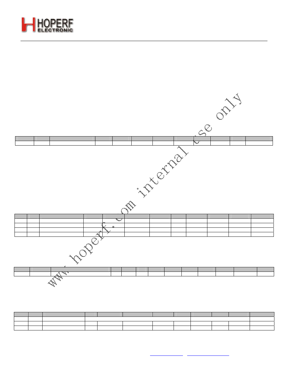
3.2.5. Device Status
Add
R/W
Function /Description
D7
D6
D5
D4
D3
D2
D1
D0
POR Def.
02
R Device
Status
ffovfl ffunfl rxffem headerr freqerr lockdet
cps[1] cps[0]
—
The operational status of the chip can be read from "Register 02h. Device Status".
3.2.6. Interrupts
The RF22 is capable of generating an interrupt signal when certain events occur. The chip notifies the microcontroller
that an interrupt event has been detected by setting the nIRQ output pin LOW = 0. This interrupt signal will be
generated when any one (or more) of the interrupt events (corresponding to the Interrupt Status bits) shown below
occur. The nIRQ pin will remain low until the microcontroller reads the Interrupt Status Register(s) (Registers 03h–04h)
containing the active Interrupt Status bit; the nIRQ output signal will then be reset until the next change in status is
detected. All of the interrupts must be enabled by the corresponding enable bit in the Interrupt Enable Registers
(Registers 05h–06h). All enabled interrupt bits will be cleared when the microcontroller reads the interrupt status
register. If the interrupt is not enabled when the event occurs inside of the chip it will not trigger the nIRQ pin, but the
status may still be read correctly at anytime in the Interrupt Status registers.
Add R/W Function/Description
D7
D6
D5
D4
D3
D2
D1
D0
POR Def.
03
R
Interrupt Status 1
ifferr
itxffafull
itxffaem irxffafull
iext
ipksent
ipkvalid
icrcerror
—
04
R
Interrupt Status 2
iswdet
ipreaval
ipreainval irssi
iwut ilbd
ichiprdy ipor
—
05 R/W
Interrupt
Enable
1
enfferr entxffafull
entxffaem enrxffafull
enext
enpksent
enpkvalid
encrcerror
00h
06 R/W
Interrupt
Enable
2
enswdet
enpreaval
enpreainval
enrssi enwut
enlbd enchiprdy
enpor 01h
See “Register 03h. Interrupt/Status 1,” on page 94 and “Register 04h. Interrupt/Status 2,” on page 97 for a complete list
of interrupts.
3.2.7. Device Code
The device version code is readable from "Register 01h. Version Code (VC)". This is a read only register.
Add
R/W
Function/Description
D7
D6
D5
D4
D3
D2
D1
D0
POR Def.
Notes
01 R
Device
Version
0 0 0 vc[4] vc[3] vc[2] vc[1] vc[0] 00h
DV
3.2.8. System Timing
The system timing for TX and RX modes is shown in Figures 2 and 3. The timing is shown transitioning from
STANDBY mode to TX mode and going automatically through the built-in sequencer of required steps. If a small range
of frequencies is being used and the temperature range is fairly constant a calibration may only be needed at the initial
power up of the device. The relevant system timing registers are shown below.
Add
R/W
Function/Description D7
D6
D5
D4
D3
D2
D1
D0
POR Def.
53 R/W
PLL
Tune
Time
pllts[4:0]
pllt0[2:0]
45h
54
R/W
Reserved
1
X
X
X
X X
X X
X 00h
55 R/W
Calibration
Control xtalstarthalf
adccaldone enrcfcal
rccal vcocaldp vcocal skipvco 04h
The VCO will automatically calibrate at every frequency change or power up. The VCO CAL may also be forced by