Rf22, Modulation data source, Fifo mode – Rainbow Electronics RF22 User Manual
Page 18: Direct mode, Pn9 mode, Synchronous vs. asynchronous
RF22
Version: 0.1 Date: 12/23/2008
Tel: +86-755-82973805 Fax: +86-755-82973550 E-mail: [email protected] http://www.hoperf.com
18
4.2. Modulation Data Source
The RF22 may be configured to obtain its modulation data from one of three different sources: FIFO mode, Direct
Mode, and from a PN9 mode. Furthermore, in Direct Mode, the TX modulation data may be obtained from several
different input pins. These options are set through the dtmod[1:0] field in "Register 71h. Modulation Mode Control 2".
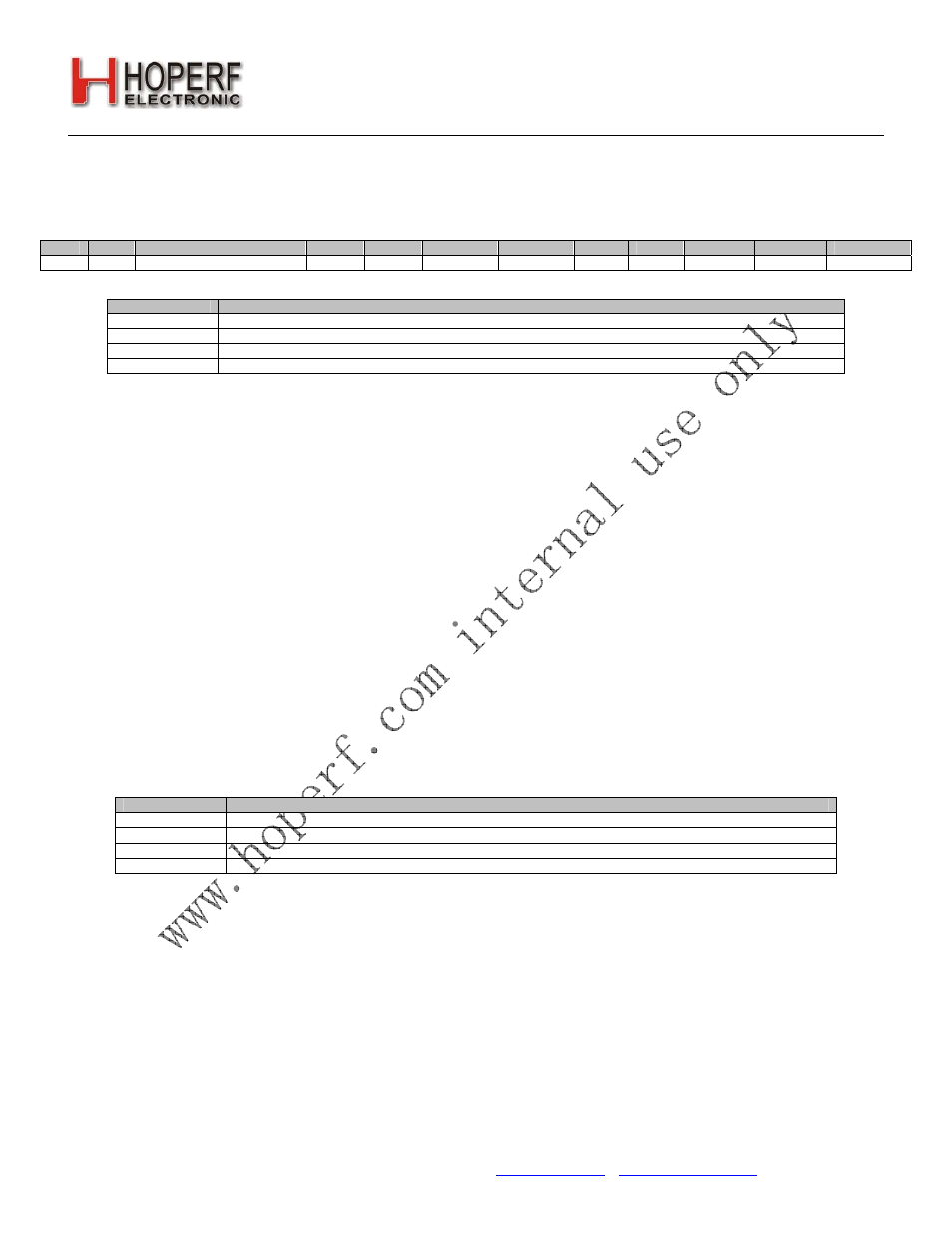
Add
R/W
Function/Description
D7
D6
D5
D4
D3
D2
D1
D0
POR Def.
71
R/W
Modulation Mode Control 2
trclk[1]
trclk[0]
dtmod[1] dtmod[0] eninv fd[8] modtyp[1]
modtyp[0]
23h
dtmod[1:0]
Modulation Source
00
Direct Mode using TX_Data via GPIO pin (GPIO needs programming accordingly also)
01
Direct Mode using TX_Data via SDI pin (only when nSEL is high)
10 FIFO
Mode
11 PN9
(internally
generated)
4.3. FIFO Mode
In FIFO mode the integrated FIFOs are used to transmit and receive the data. The FIFOs are accessed via "Register
7Fh. FIFO Access" with burst read/write capability. The FIFOs may be configured specific to the application packet size,
etc. (see "6. Data Handling and Packet Handler" on page 39 for further information). When in FIFO mode the chip will
automatically exit TX or RX State when either the ipksent or ipkvalid interrupt occurs. The chip will return to any of
other states based on the settings in "Register 07h. Operating Mode and Function Control 1". For instance if the chip is
put into TX mode and both the txon and pllon bits are set, the chip will transmit all of the contents of the FIFO and the
ipksent interrupt will occur. When this event occurs the chip will clear the txon bit and return to pllon or Tune Mode. If
no other bits are set in register 07h besides txon initially then the chip will return to the Idle state.
In RX mode the rxon bit will only be cleared if ipkvalid occurs. A CRC, Header, or Sync error will generate an interrupt
and the microcontroller will need to decide on the next action.
4.4. Direct Mode
For legacy systems that have packet handling within an MCU or other baseband chip, it may not be desirable to use
the FIFO. For this scenario, a Direct Mode is provided which bypasses the FIFOs entirely. In Direct Mode the TX
modulation data is applied to an input pin of the chip and processed in “real time” (i.e., not stored in a register for
transmission at a later time). There are various configurations for choosing which pin is used for the TX Data.
Furthermore, an additional input pin is required for the TX Data Clock if GFSK modulation is desired (only the TX Data
input pin is required for FSK). Two options for the source of the TX Data are available in the dtmod[1:0] field, and
various configurations for the source of the TX Data Clock may be selected through the trclk[1:0] field.
trclk[1:0]
TX Data Clock Configuration
00
No TX Clock (only for FSK)
01
TX Data Clock is available via GPIO (GPIO needs programming accordingly as well)
10
TX Data Clock is available via SDO pin (only when nSEL is high)
11
TX Data Clock is available via the nIRQ pin
The eninv bit in Address 71h will invert the TX Data for testing purposes.
4.5. PN9 Mode
In this mode the TX Data is generated internally using a pseudorandom (PN9 sequence) bit generator. The primary
purpose of this mode is for use as a test mode to observe the modulated spectrum without having to load/provide data.
4.6. Synchronous vs. Asynchronous
In Asynchronous mode no clock is used to synchronize the data to the internal modulator. This mode can only be used
with FSK. The advantage of this mode that it saves a microcontroller pin because no data clock is required. The
disadvantage is that you don’t get the clean spectrum and limited BW of GFSK. If Asynchronous FSK is used the
TX_DR register should be set to its maximum value.