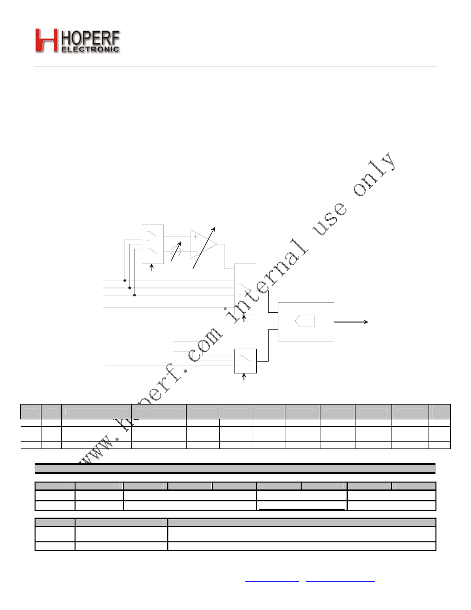
Rf22, General purpose adc, Figure 23. general purpose adc architecture – Rainbow Electronics RF22 User Manual
Page 35
RF22
Version: 0.1 Date: 12/23/2008
Tel: +86-755-82973805 Fax: +86-755-82973550 E-mail: [email protected] http://www.hoperf.com
35
8.3. General Purpose ADC
An 8-bit SAR ADC is integrated onto the chip for general purpose use, as well as for digitizing the temperature sensor
reading. “Register 0Fh. ADC Configuration,” on page 56 must be configured depending on the use of the GP ADC
before use. The architecture of the ADC is demonstrated in Figure 23. First the input of the ADC must be selected by
setting the ADCSEL[2:0] depending on the use of the ADC. For instance, if the ADC is going to be used to read out the
internal temperature sensor, then ADCSEL[2:0] should be set to 000. Next, the input reference voltage to the ADC
must be chosen. By default, the ADC uses the bandgap voltage as a reference so the input range of the ADC is from
0–1.02 V with an LSB resolution of 4 mV (1.02/255). Changing the ADC reference will change the LSB resolution
accordingly.
Every time the ADC conversion is desired, the ADCStart bit in "Register 0Fh. ADC Configuration" must be set to 1. This
is a self clearing bit that will be cleared at the end of the conversion cycle of the ADC. The conversion time for the ADC
is 350 us. After the 350 us or when the ADCstart/busy bit is cleared, then the ADC value may be read out of "Register
11h. ADC Value". Setting the "Register 10h. ADC Sensor Amplifier Offset", ADC Sensor Amplifier Offset is only
necessary when the ADC is configured to used as a Bridge Sensor as described in the following section.
……
……
……
Diff. MUX
Diff. Amp.
Input MUX
Ref MUX
Vin
Vref
……
ADCSEL<2:0>
OTR<3:0>
GAIN<1:0>
ADCSEL<2:0>
REFSEL<1:0>
VMEAS<7:0>
VBAT/3
VBAT/2
GPIO1
GPIO0
GPIO2
TS
VBG(1.2V)
8-bit ADC
0-1020mV / 0-255
Figure 23. General Purpose ADC Architecture
Add R/W Function/Description
D7
D6
D5
D4
D3
D2
D1
D0
POR
Def.
0F R/W ADC Configuration
adcstart/adcbusy adcsel[2] adcsel[1] adcsel[0] adcref[1] adcref[0]
adcgain[1] adcgain[0] 00h
10 R/W ADC Sensor Amplifier
Offset
adcoffs[3]
adcoffs[2]
adcoffs[1] adcoffs[0] 00h
11
R ADC Value
adc[7]
adc[6]
adc[5]
adc[4]
adc[3]
adc[2]
adc[1]
adc[0]
—
Register 0Fh. ADC Configuration
Bit
D7
D6
D5
D4
D3
D2
D1
D0
Name
adcstart/adcdone
adcsel[2:0]
adcref[1:0]
adcgain[1:0]
Type R/W
R/W
R/W
R/W
Reset value = 00000000
Bit
Name
Function
7
adcstart/adcdone
ADC Measurement Start Bit.
Reading this bit gives 0 if the ADC measurement cycle has been finished.
6:4
adcsel[2:0]
ADC Input Source Selection.