Rf22 – Rainbow Electronics RF22 User Manual
Page 41
RF22
Version: 0.1 Date: 12/23/2008
Tel: +86-755-82973805 Fax: +86-755-82973550 E-mail: [email protected] http://www.hoperf.com
41
[ ]
(
)
ms
D
R
ldc
TLDC
768
.
32
32
2
0
:
7
Ч
−
Ч
Ч
=
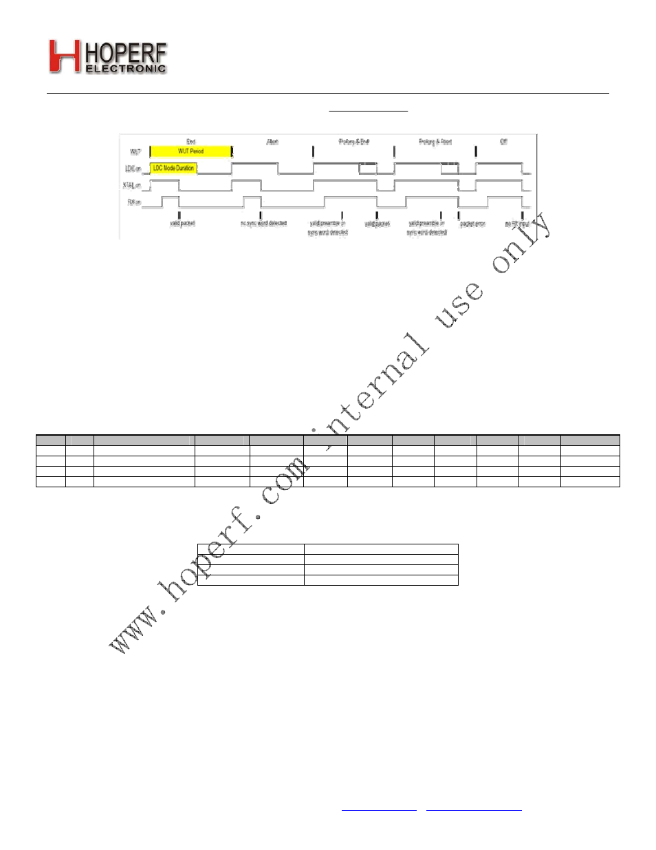
Figure28. Low Duty Cycle Mode
8.8. GPIO Configuration
Three general purpose IOs (GPIOs) are available. Numerous functions such as specific interrupts, TRSW control,
Antenna Diversity Switch control, Microcontroller Output, etc. can be routed to the GPIO pins as shown in the tables
below. When in Shutdown mode all the GPIO pads are pulled low.
Note: The ADC should not be selected as an input to the GPIO in Standby or Sleep Modes and will cause excess current
consumption.
Add R/W Function/ Description D7
D6
D5
D4
D3
D2
D1
D0
POR Def.
0B R/W GPIO0 Configuration
gpio0drv[1] gpio0drv[0]
pup0
gpio0[4]
gpio0[3] gpio0[2] gpio0[1] gpio0[0]
00h
0C R/W GPIO1 Configuration
gpio1drv[1] gpio1drv[0]
pup1
gpio1[4]
gpio1[3] gpio1[2] gpio1[1] gpio1[0]
00h
0D R/W GPIO2 Configuration
gpio2drv[1] gpio2drv[0]
pup2
gpio2[4]
gpio2[3] gpio2[2] gpio2[1] gpio2[0]
00h
0E R/W I/O Port Configuration
extitst[2]
extitst[1] extitst[0] itsdo
dio2
dio1
dio0
00h
The GPIO settings for GPIO1 and GPIO2 are the same as for GPIO0 with the exception of the 00000 default setting.
The default settings for each GPIO are listed below:
GPIO
00000—Default Setting
GPIO0
POR
GPIO1
POR Inverted
GPIO2
Microcontroller Clock
The diagrams in Figure 29 show two different configurations/usage of the GPIO. In Configuration A an external sensor
is used and the GPIO is configured as an input with the 00101 External Interrupt, Rising Edge setting. When the sensor
is triggered the nIRQ pin will go high and the microcontroller will be able to read the interrupt register and know that an
event occurred on the sensor. The advantage of this configuration is that it saves a microcontroller pin. This application
utilizes the high output power so a TRSW is required.
In Configuration B, the chip is configured to provide the System Clock output to the microcontroller so that only one
crystal is needed in the system, therefore reducing the BOM cost. For the TX Data Source, Direct Mode is used
because long packets are desired with a unique packet handling format already implemented in the microcontroller. In
this configuration the TX Data Clock is configured onto GPIO0, the TX Data is configured onto GPIO1, and the
Microcontroller System Clock output is configured onto GPIO2. In this application only the lowest output power setting
is required so no TRSW is needed.
For a complete list of the available GPIO's see “Register 0Ch. GPIO Configuration 1,” on page 107, “Register 0Dh.
GPIO Configuration 2,” on page 108, and “Register 0Eh. I/O Port Configuration,” on page 109.