Direct rdram* reference voltage, High-speed cmos routing, Figure 32. ramref generation example circuit – Intel CHIPSET 820E User Manual
Page 54
Intel
®
820E Chipset
R
54
Design
Guide
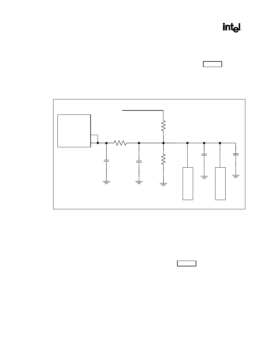
2.7.3.
Direct RDRAM* Reference Voltage
The Direct RDRAM reference voltage (RAMREF) must be generated as shown in Figure 32. The
RAMREF should be generated from a typical resistor divider using 2%-tolerance resistors. Additionally,
the RAMREF must be decoupled locally at each RIMM connector, at the resistor divider, and at the
MCH. Finally, as shown in Figure 32, a 100
Ω
series resistor is required near the MCH. The RAMREF
signal should be routed with a 10 mil-wide trace.
Figure 32. RAMREF Generation Example Circuit
160
Ω
2%
R
I
M
M
V
TERM
R3
C4
C10
C5
C8
0.1 µF
0 .1 µF
100
Ω
R1
R2
0.1 µF
0.1 µF
R
I
M
M
ramref_generation.vsd
560
Ω
2%
RAMREFA
RAMREFB
MCH
2.7.4.
High-Speed CMOS Routing
•
The high-speed CMOS signals (CMD & SCK) must be routed using 28
Ω
traces. Using the
recommended stack-up, these signals will be 18 mils wide.
•
The high-speed CMOS signals must be length-matched to the RSL signals within 1200 mils
(1.2 inches), because of a timing requirement between CMOS and RSL signals during NAP Exit and
PDN Exit.
•
The high-speed CMOS signals require termination as shown in Figure 33, as a result of the buffer
strengths in the MCH.
•
The resistors must be 91
Ω
pull-up and 39
Ω
pull-down, and they must be 2% or better for S3 mode
reliability. The trace impedances remain 28
Ω
.