Vref guard band, Ringback levels, Overdrive region – Intel CHIPSET 820E User Manual
Page 161: Guard band, Figure 84. overdrive region and v
Intel
®
820E Chipset
R
Design Guide
161
3.5.1. V
REF
Guard Band
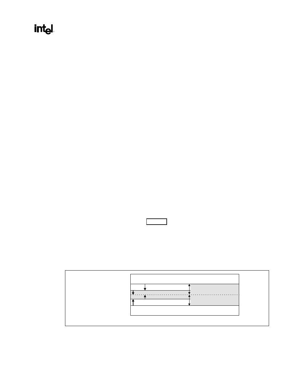
To account for noise sources that may affect the way an AGTL+ signal becomes valid at a receiver, V
REF
is shifted by
∆
V
REF
for measuring the minimum and maximum flight times. The V
REF
guard band region
is bounded by V
REF
–
∆
V
REF
and V
REF
+
∆
V
REF
.
∆
V
REF
has a value of 100 mV, which accounts for the
following noise sources:
•
Motherboard coupling
•
V
TT
noise
•
V
REF
noise
3.5.2. Ringback
Levels
The example topology covered in this guideline assumes a ringback tolerance allowed to within 200 mV
of 2/3 V
TT
. Since V
TT
is specified with an approximate total tolerance of ±11%, this implies a 2/3 V
TT
(V
REF
) range, from approximately 0.89 V to 1.11 V. This sets the absolute ringback limits as follows:
•
1.3 V (1.1 V + 200 mV) for rising-edge ringback
•
0.69 V (0.89 V – 200 mV) for falling-edge ringback
A violation of these ringback limits requires flight time correction as documented in the Intel
®
Pentium
®
III Processor Developer’s Manual.
3.5.3. Overdrive
Region
The overdrive region is the voltage range at a receiver, from V
REF
to V
REF
+ 200 mV, for a low-to-
high-going signal, and from V
REF
to V
REF
– 200 mV for a high-to-low-going signal. The overdrive
regions encompass the V
REF
guard band, so when V
REF
is shifted by
∆
V
REF
for timing measurements, the
overdrive region does not shift by
∆
V
REF
. Figure 84 depicts this relationship. Corrections for edge rate
and ringback are documented in the Intel
®
Pentium
®
II Processor Developer’s Manual. However, there is
an exception to the documented correction method: The Intel
®
Pentium
®
III Processor Developer’s
Manual states that extrapolations should be made from the last crossing of the overdrive region back to
V
REF
. Simulations performed on this topology should extrapolate back to the appropriate V
REF
guard
band boundary, and not to V
REF
. So, for maximum rising-edge correction, extrapolate back to V
REF
+
∆
V
REF
. For maximum falling-edge corrections, extrapolate back to V
REF
–
∆
V
REF
.
Figure 84. Overdrive Region and V
REF
Guard Band
overdrive_vref_guard
V
REF
+ 200 mV
∆
∆∆
∆
∆
∆∆
∆
V
REF
+ 100 mV
V
REF
V
REF
- 100 mV
V
REF
- 200 mV
V
REF
V
REF
V
REF
Guardband
Overdrive Region (200 mV)
Overdrive Region (200 mV)