Table 56. intel, 820e chipset platform clock skews – Intel CHIPSET 820E User Manual
Page 165
Intel
®
820E Chipset
R
Design Guide
165
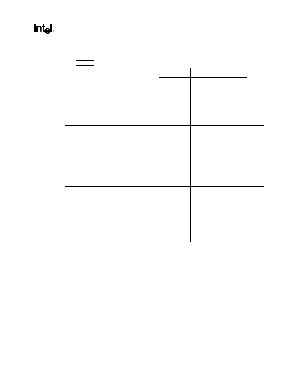
Table 56. Intel
®
820E Chipset Platform Clock Skews
Clock Symbols (see
Relationship Skew
Notes
Pin-to-Pin (ps)
Board (ps)
Total (ps)
Min. Max. Min. Max. Min. Max.
A leads C
A leads E
(or C leads E)
PGA370 HCLK to PGA370
HCLK (DP only)
and
PGA370 HCLK to MCH
HCLK (DP only)
-175 +175 -125 +125 -300 +300 1,
7
A leads E
PGA370 HCLK to MCH HCLK
(UP only)
0
0 -125 +125 -125 +125 2,
3,
7
P leads F
MCH CLK66 to AGP graphics
device AGPCLK
0
0 -125 +125 -125 +125 4,
8
L leads another L
(or L leads H)
PCICLK to PCICLK
-500
+500 -1500 +1500 -2000 +2000
I leads H
ICH2 CLK66 leads ICH2
PCICLK
+1500 +4000
-500 +500 +1000 +4500
F leads I
ICH2 CLK66 to MCH CLK66
-250
250
-125
+125
-375
+375
8
Worst-case skew
between H, L, M, and
N
Worst-case FWHCLK,
LPCCLK, PCICLK
-500 +500 -1500 +1500 -2000 +2000
5
B leads D
B leads G
processor PICCLK leads
processor PICCLK
and
processor PICCLK leads
ICH2 APICCLK
-250 +250 -125 +125 -375 +375 6
NOTES:
1. DP only
2. UP: MCH and processor clock drivers are tied together to eliminate pin-to-pin skew. -175 and +175 pin-to-pin
skew apply only to DP.
3. UP only
4. Clock drivers tied together to eliminate pin-to-pin skew.
5. The skew between any PCICLK clocks on any two inputs in the system
6. The skew between any APIC clocks on any two inputs in the system
7. If SSC is enabled, an additional ±40 ps must be added to the pin-to-pin skew.
8. If SSC is enabled, an additional ±60 ps must be added to the pin-to-pin skew.