Table 49. ck-sks clocking, Table 50. rtc – Intel CHIPSET 820E User Manual
Page 137
Intel
®
820E Chipset
R
Design Guide
137
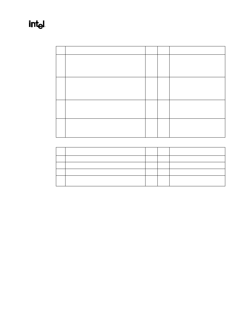
Table 49. CK-SKS Clocking
# Layout
Recommendations Yes
No Comments
1
CLK_33 goes to ICH2, FWH FLASH BIOS, and
SIO.
Clock chip to series resistor = 0.5 inch, and from
series resistor to receiver = 15 inches max.
Routed on one layer.
2
PCI_33 goes to PCI device or PCI slot. There are 5
clocks.
Clock chip to series resistor = 0.5 inch, and from
series resistor to receiver = 13 inches max.
Routed on one layer.
3
CLK_66 goes to ICH2 and MCH.
Clock chip to series resistor = 0.5 inch, and from
series resistor to receiver = 14 inches max.
Routed on one layer.
4
AGP_66 goes to AGP connector.
Clock chip to series resistor = 0.5 inch, and from
series resistor to receiver = 11 inches max.
Routed on one layer.
Table 50. RTC
# Layout
Recommendations Yes
No Comments
1
RTC lead length
≤
0.25 inch max.
2
Minimize capacitance between Xin and Xout.
3
Put GND plane underneath crystal components.
4
Don’t route switching signals under external
components (unless on other side of board).