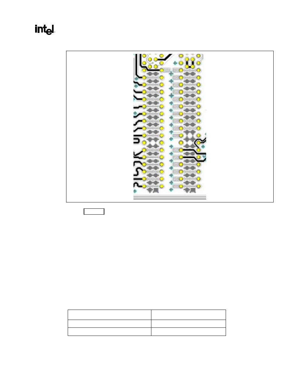
Enhancement recommendation, Figure 25. section b (see note), bottom layer – Intel CHIPSET 820E User Manual
Page 47

Intel
®
820E Chipset
R
Design Guide
47
Figure 25. Section B (See Note), Bottom Layer
Note: Refer to Figure 21. For clarity, the ground flood was removed from the picture.
2.7.2.4.1. Direct RDRAM* Channel Connector Compensation Enhancement
Recommendation
From further analysis, it was determined that the amount of capacitance needed for RSL traces depends
on the lengths that the signals have to travel though the RIMM connector pin. (i.e., a signal on the bottom
layer has to travel through more of the RIMM connector pin than a signal on the top layer). As a result of
the travel through the pin, signals routed on the bottom layer have a larger inductance at the connector,
which causes a larger impedance discontinuity, resulting in a possible reduction of voltage and timing
margin on those signals. As a result, RSL traces on the bottom layer need more capacitive compensation
than RSL traces routed on the top layer. RSL signals routed on the bottom layer need 0.55 pF more
compensation than signals routed on the top layer. To compensate for the inductance of the connector,
approximately 0.65 pF to 0.85 pF compensating capacitive tabs (C-TAB) are required for each topside
RSL trace, and approximately 1.20 pF – 1.4 pF is required for each bottom-side RSL trace.
Table 5. RSL and Clocking Signal RIMM Connector Capacitance Recommendations
RSL and Clocking Signal Routing Layer
Capacitance (pF)
Top
0.65 – 0.85
Bottom
1.20 – 1.40
