Table 32. gpio, Table 33. usb interface – Intel CHIPSET 820E User Manual
Page 128
Intel
®
820E Chipset
R
128
Design
Guide
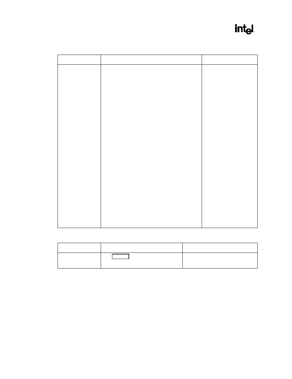
Table 32. GPIO
Checklist Items
Recommendations
Reason/Effect
GPIO pins
GPIO[0:7]:
•
These pins are in the main power well. Pull-ups must
use the 3.3 V plane.
•
Unused core well inputs must either be pulled up to
VCC3.3 or be pulled down. These inputs must not be
allowed to float.
•
GPIO[1:0] can be used as REQ[A:B]#.
•
GPIO[1] also can be used as PCI REQ[5]#.
•
These signals are 5 V tolerant.
Ensure that all unconnected
signals are outputs only!
GPIO[8] & [11:13]:
•
These pins are in the resume power well. Pull-ups
must use the VCCSUS3.3 plane.
•
Unused resume well inputs must be pulled up to
VCCSUS3.3.
•
These are the only GPIs that can be used as ACPI-
compliant wake events.
•
These signals are not 5 V tolerant.
These are the only GPI
signals in the resume well
with associated status bits in
the GPE1_STS register.
GPIO[16:23]:
•
Fixed as output only. Can be left NC.
•
In the main power well
•
GPIO22 is open-drain.
GPIO[24, 25, 27, 28]:
•
I/O pins. Can be left NC.
•
From resume power well
Table 33. USB Interface
Checklist Items
Recommendations
Reason/Effect
USBP[3:0]P
USBP[3:0]N
See Figure 56 for the circuitry needed on
each differential pair.