Thermal design power, Glue chip 3 (intel® 820e chipset glue chip), Glue chip 3 (intel – Intel CHIPSET 820E User Manual
Page 193: 820e chipset glue chip), Table 63. intel, 820e chipset component thermal design power
Intel
®
820E Chipset
R
Design Guide
193
6.3.
Thermal Design Power
The thermal design power is the estimated maximum possible expected power generated in a component
by a realistic application. It is based on extrapolations of both hardware and software technology over the
life of the product. It does not represent the expected power generated by a power virus. For thermal
design considerations regarding the Pentium III processor using the Intel PGA370 socket, refer to the
Intel
®
820 Chipset Design Guide Addendum for the Intel
®
Pentium
®
III Processor for the PGA370
Socket. These guidelines can be downloaded from the Intel website at:
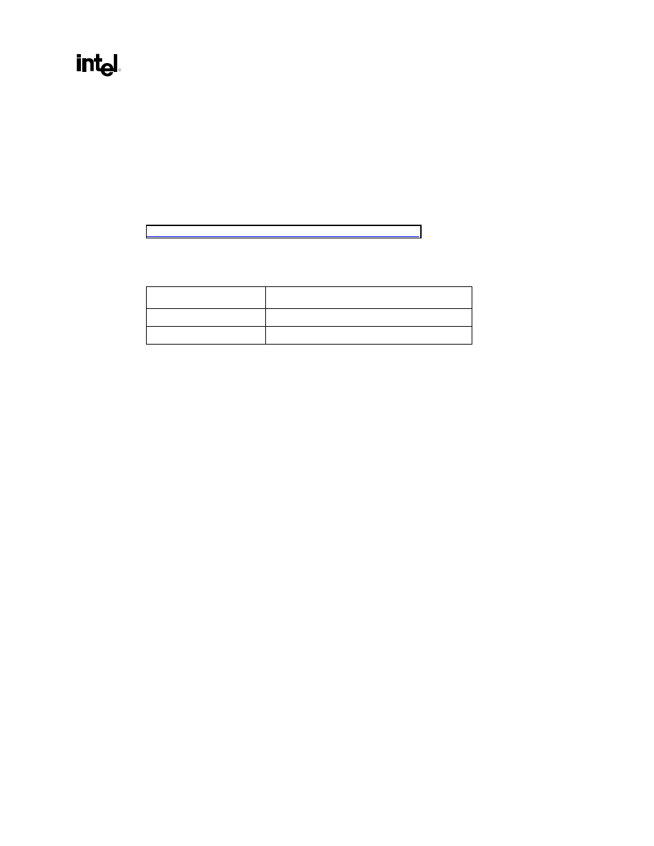
The thermal design power numbers for the MCH and the ICH2 are listed in the following table.
Table 63. Intel
®
820E Chipset Component Thermal Design Power
Component
Thermal Design Power (133/400 MHz)
MCH
3.5 W ± 15%
ICH2
1.5 W ± 15%
6.4.
Glue Chip 3 (Intel
®
820E Chipset Glue Chip)
To reduce the component count and BOM cost of the Intel 820E chipset platform, Intel has developed an
ASIC component that integrates miscellaneous platform logic into a single chip. Glue Chip 3 is designed
to integrate some or all of the following functions into a single device. By integrating much of the
required glue logic into a single device, the overall board cost can be reduced.
Features
•
PWROK signal generation
•
Control circuitry for Suspend to RAM
•
Power supply power-up circuitry
•
RSMRST# generation
•
Back-feed cutoff circuit for Suspend to RAM
•
5 V reference generation
•
Flash FLUSH# / INIT# circuit
•
HD single-color LED driver
•
IDE reset signal generation/PCIRST# buffers
•
Voltage translation for audio MIDI signal
•
Audio disable circuit
•
Voltage translation for DDC to monitor
•
Tri-state buffers for test