Maxim Integrated MAXQ622 User Manual
Page 85
MAXQ612/MAXQ622 User’s Guide
5-12
Maxim Integrated
REGISTER
DESCRIPTION
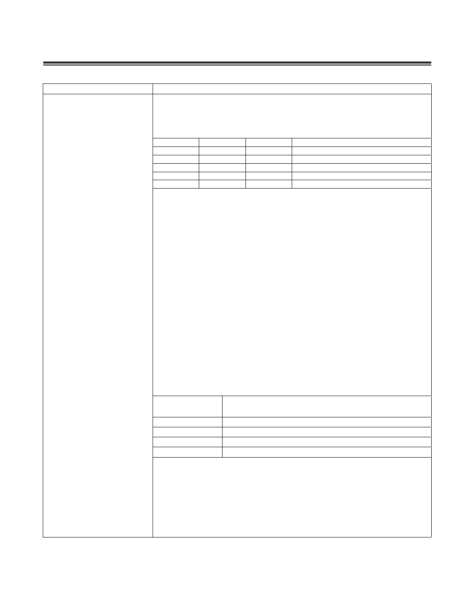
PWCN.4 (IRTXOE)
IRTX Output Enable. The IRTXOE bit is used in conjunction with the IRTXOUT bit to
determine the state of the IRTX pin when the IR timer is not enabled (i .e ., IREN = 0) . When
the bit is set to 1, the IRTX pin is used as an output; data in the IRTXOUT bit is driven on
the pin . When the bit is cleared to 0, the IRTX pin is three-stated (if IRTXOUT = 0) or weakly
pulled up (if IRTXOUT = 1) .
IRTXOE
IRTXOUT
IREN
IRTX PIN STATE
0
0
0
High-Z
0
1
0
Weak Pullup
1
0
0
Strong 0
1
1
0
Strong 1
X
X
1
IR Timer Tx Control
PWCN.5 (IRTXOUT)
IRTX Output Pin Control. This bit controls the output drive state for the IRTX pin when the
IR timer is not enabled (i .e ., IREN = 0) and when the IRTX pin has been enabled for output
by IRTXOE = 1 . When IREN = 0 and IRTXOE = 1, setting this bit to 1 enables a strong
output high drive on the IRTX pin . Clearing this bit to 0 enables a strong output low drive on
the IRTX pin . When IRTXOE = 0 and the IR timer is not enabled (IREN = 0), this bit controls
the input mode for the IRTX pin . When IRTXOE = 0, the IRTX pin is three-state . When
IRTXOE = 1, the pin is weakly pulled up .
PWCN.6 (IRRXWP)
IRRX Weak Pullup Enable. This bit controls the input mode of the IRRX pin . When this bit
is set to 1, the internal weak pullup is enabled . When this bit is cleared to 0, the internal
weak pullup is turned off, resulting in the three-state input mode .
PWCN.7 (PFRST)
Power-Fail Reset Flag. This bit is set to 1 whenever a power-fail reset occurs . It is
unaffected by other forms of reset . This bit can be checked by software following a reset to
determine if it was a power-fail reset that occurred . It should always be cleared by software
following a reset to ensure that the source of any future reset can be determined correctly .
Note that this bit is set anytime V
DD
< V
RST
. The WDCN .POR bit can be examined to
determine whether V
DD
was below the V
POR
threshold .
PWCN.9 to PWCN.8 (PFRCK[1:0])
Power-Fail Reset Check Time Bits 1:0. These bits are used to enable duty cycling of the
V
RST
power-monitoring circuitry during the time when V
DD
is below the V
RST
threshold, but
has not reached the POR threshold . The duty cycling of the power-fail monitor during the
V
RST
condition is provided to reduce the time-averaged current consumption and extend
the SRAM data-retention time when the battery voltage is low, but still provide adequate
response time to exit the V
RST
state if the battery source is replaced . These bits are reset
only by POR (not even V
RST
) . The table below provides the bit settings and corresponding
duty cycling of the power monitor check when V
POR
< V
DD
< V
RST
.
PFRCK[1:0]
POWER-FAIL MONITOR CHECK INTERVAL (NANOPOWER RING
OSCILLATOR CYCLES)
00
No interval defined (Monitor on always as normal)
01
2
10
(~128ms for 8kHz nanopower ring oscillator frequency)
10
2
11
(~256ms for 8kHz nanopower ring oscillator frequency)
11
2
12
(~512ms for 8kHz nanopower ring oscillator frequency)
PWCN.10 (FRCVDD)
Force V
DD
Power Supply. When set to 1, V
DDB
power switching is disabled, and V
DD
is
always used as the core 3V power supply . When this bit is cleared to 0, V
DDB
is used as
the core 3V supply if V
BUS
is present . This bit is cleared on all reset .
PWCN.11 (CTMS)
System Clock Multiplier Select. When set to 1, this bit selects the output of the USB clock
multiplier PLL as the source of the system clock (the switchover occurs when CKRY is
high) . The USB PLL is enabled whenever the USB is enabled or when this bit is set . The
output of the PLL is 48MHz (12MHz crystal input x 4), which is then automatically divided
by 4 to provide the system clock with a 12MHz clock, synchronous to the USB clock . When
cleared, the USB PLL is enabled or disabled by the USB enable .