2 master-receiver, 3 slave-transmitter, 11 .1 .2 master-receiver -4 – Maxim Integrated MAXQ622 User Manual
Page 159: 11 .1 .3 slave-transmitter -4, Figure 11-4 . i, C master-receiver data transfer -4
MAXQ612/MAXQ622 User’s Guide
11-4
Maxim Integrated
11.1.2 Master-Receiver
When operating in master mode with I2CMODE bit set to 1, the I
2
C module is operating in master-receiver mode . The
I
2
C operates in a similar fashion as in master-transmitter mode . The master initiates the transfer by generating the
START condition . Once START has been successfully generated, the master transmits the slave address (I2CBUF)
according to address setting (I2CEA) . Note that in the first part of the transfer, the master acts as a transmitter so
that it can address the targeted I
2
C slave device on the bus . Therefore, on completion of address transfer, it sets the
transmit complete flag (I2CTXI = 1) . After the master has successfully addressed the target, the master then switches
to receiver mode . The master starts outputting SCL receiving clock pulses and shifting in data from SDA unless clock
stretching is enabled .
Once the master has received a data byte from the slave, it loads the data into I2CBUF and sets I2CRXI = 1 . This also
generates an interrupt to the CPU if the receive ready interrupt is enabled (I2CRXIE = 1) . The CPU can then read data
from the I2CBUF .
Meanwhile, the master continues to output receiver clock because the I2CBUF is double-buffered on receive . This
allows the I
2
C module to continue receiving data while the previous data byte is being processed . If the second byte
is received before the first byte is read (the CPU has not read the I2CBUF yet), the second byte is not copied into the
I2CBUF . Instead, the I
2
C receive overrun flag is set (I2CROI = 1) . This generates a receive overrun interrupt to the
CPU if enabled . Meanwhile, the I
2
C controller responds to the transmitter with the I2CACK value . The master does not
output any more receiver clock pulses unless the I2CROI flag is cleared to 0 .
The I2CROI flag can only be cleared by CPU reading I2CBUF . On clearing the I2CROI flag, the I
2
C controller also
loads the second byte into I2CBUF and generates an I
2
C receive interrupt if enabled . The receiver then resumes its
operation . The master outputs receiver clock pulses after satisfying the SCL low time requirement .
At the end of the each data byte received, the master acknowledges according to the setting of the I2CACK bit . When
the I2CACK bit is set to 1, the master leaves SDA high and acknowledges with a NACK (A) . When the I2CACK bit is
cleared to 0, the master pulls SDA low . A NACK from the master indicates to the slave that the master has received all
the bytes it expects from the slave, and the slave should release the SDA line on the following SCL low and allow the
master to drive the SDA line to generate a STOP or START condition .
11.1.3 Slave-Transmitter
The I
2
C module functions as a slave-transmitter when an address match is identified (I2CAMI = 1) and the R/W bit is
1 . On detecting a START (S) condition, the I
2
C controller, if enabled, shifts in the address bits and compares it against
its own address (I2CSLA) . If the address matches, the I2CAMI flag is set to 1 and an interrupt is generated if enabled .
The I2CMST master mode bit is cleared to 0 and the I2CMODE transfer mode bit is updated with the received R//W
bit value of 1, indicating that the master wants to read from the slave and the slave operates as the transmitter . On
detecting this, the I
2
C controller operates in slave-transmitter mode . The I
2
C module shifts out the I
2
C transmit buffer
content when the master starts clocking the SCL . On completion of transmitting a data byte, the I
2
C controller sets the
transmit complete flag to 1 (I2CTXI) and generates an interrupt if enabled .
If the master expects no more data from the slave, it sends a NACK as the acknowledgement . On receiving the NACK,
the I
2
C controller must release the SDA line so that the external master can drive SDA in the next clock period .
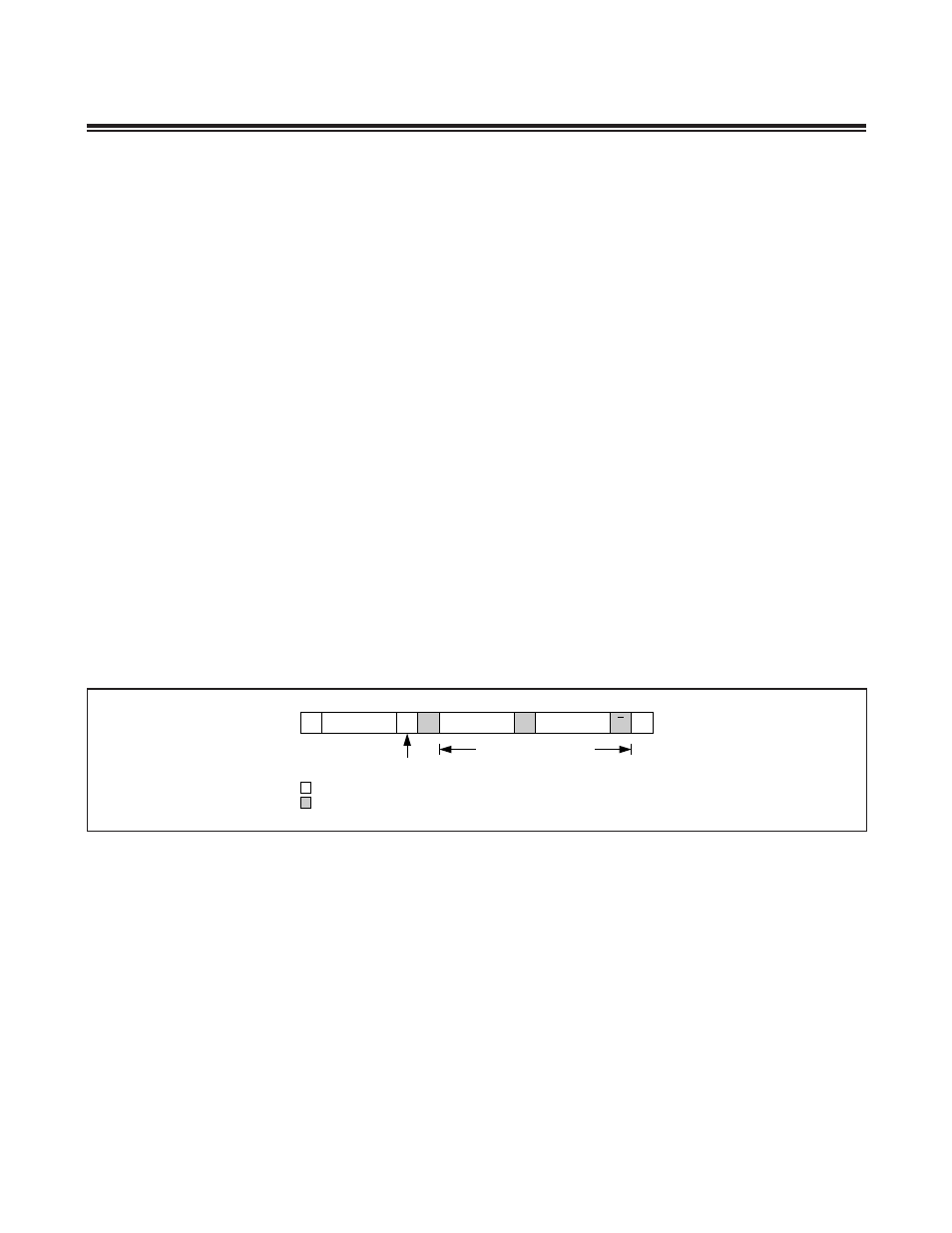
Figure 11-4. I
2
C Master-Receiver Data Transfer
S
DATA
1
SLAVE ADDR
A
P
A
DATA
A
READ
MASTER TO SLAVE
SLAVE TO MASTER
DATA TRANSFERRED
(n BYTES + ACKNOWLEDGE)