5 i2c clock control register (i2cck), 6 i2c timeout register (i2cto), 11 .4 .5 i – Maxim Integrated MAXQ622 User Manual
Page 167: C clock control register (i2cck) -12, 11 .4 .6 i, C timeout register (i2cto) -12, C clock control register (i2cck), C timeout register (i2cto)
MAXQ612/MAXQ622 User’s Guide
11-12
Maxim Integrated
11.4.5 I
2
C Clock Control Register (I2CCK)
Bits 15 to 8: I
2
C Clock High (I2CCKH[7:0]). These bits define the I
2
C SCL high period in number of system clock, with
bit 7 as the most significant bit . The duration of SCL high time is calculated using the following equation:
I
2
C High Time Period = System Clock x (I2CCKH[7:0] + 1)
When operating in master mode, the I2CCKH must be set to a minimum value of 2 to ensure proper operation . Any
value less than 2 is set to 2 .
Bits 7 to 0: I
2
C Clock Low (I2CCKL[7:0]. These bits define the I
2
C SCL low period in number of system clock, with
bit 7 as the most significant bit . The duration of SCL low time is calculated using the following equation:
I
2
C Low Time Period = System Clock x (I2CCKL[7:0] + 1)
When operating in master mode, the I2CCKL must be set to a minimum value of 4 to ensure proper operation . Any
value less than 4 is set to 4 .
11.4.6 I
2
C Timeout Register (I2CTO)
Bits 7 to 0: I
2
C Timeout Register (I2CTO[7:0]). This register is used only in master mode . This register determines
the number of I
2
C Bit Period (SCL High + SCL Low) the I
2
C master waits for SCL to go high . The timeout timer resets
to 0 and starts to count after the I2CSTART bit is set or every time the SCL goes low . When cleared to 00h, the time-
out function is disabled and the I
2
C waits for SCL to go high indefinitely during a transmission . When set to any other
values, the I
2
C waits until the timeout expires and sets the I2CTOI flag .
I
2
C Timeout = I
2
C Bit Rate x (I2CTO[7:0] + 1)
Note that these bits have no effect when the I
2
C module is operating in slave mode (I2CMST = 0) . When operating in
slave mode, SCL is controlled by an external master .
Note 1: Writes to this register are ignored when I2CBUSY = 0.
Note 2: This register has no function in slave mode.
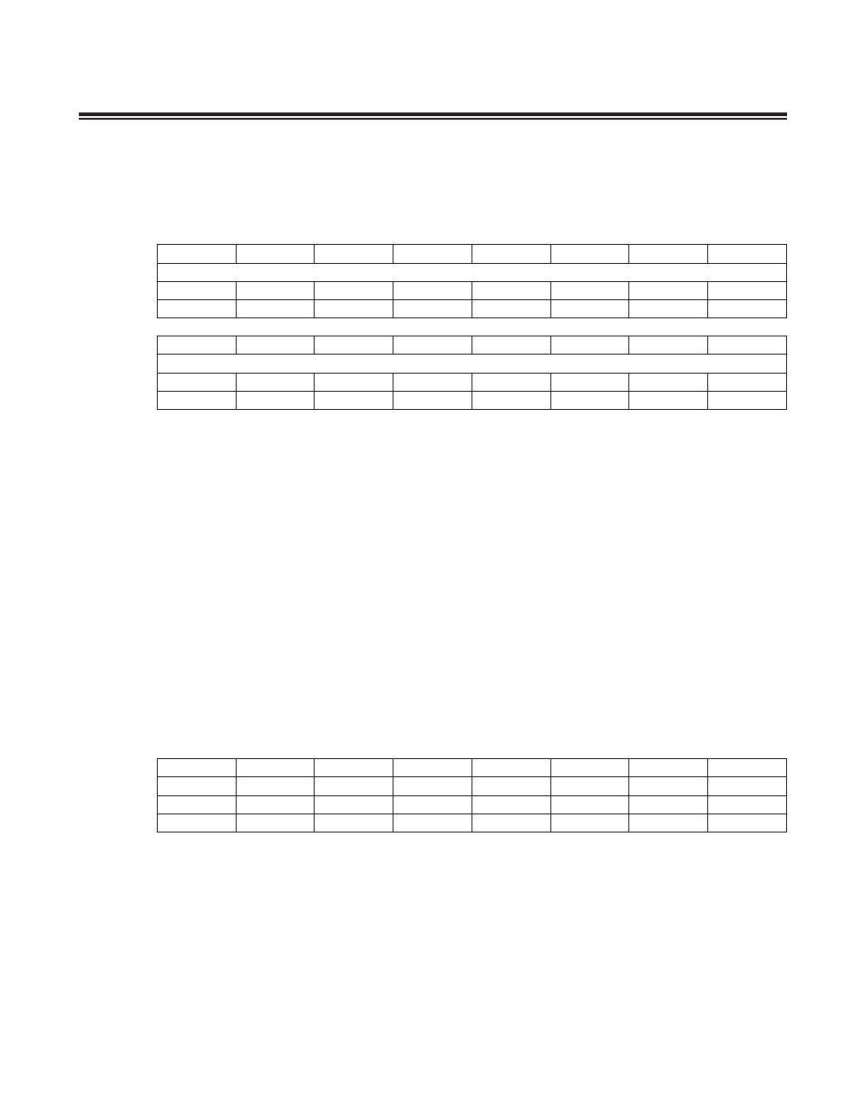
Register Name
I2CCK
Register Description
I
2
C Clock Control Register
Register Address
M4[08h]
Register Name
I2CTO
Register Description
I
2
C Timeout Register
Register Address
M4[09h]
Bit #
15
14
13
12
11
10
9
8
Name
I2CCKH[7:0]
Reset
0
0
0
0
0
0
1
0
Access
rw
rw
rw
rw
rw
rw
rw
rw
Bit #
7
6
5
4
3
2
1
0
Name
I2CCKL[7:0]
Reset
0
0
0
0
0
1
0
0
Access
rw
rw
rw
rw
rw
rw
rw
rw
Bit #
7
6
5
4
3
2
1
0
Name
I2CTO7
I2CTO6
I2CTO5
I2CTO4
I2CTO3
I2CTO2
I2CTO1
I2CTO0
Reset
0
0
0
0
0
0
0
0
Access
rw
rw
rw
rw
rw
rw
rw
rw