Maxim Integrated MAXQ622 User Manual
Page 109
MAXQ612/MAXQ622 User’s Guide
Maxim Integrated
6-7
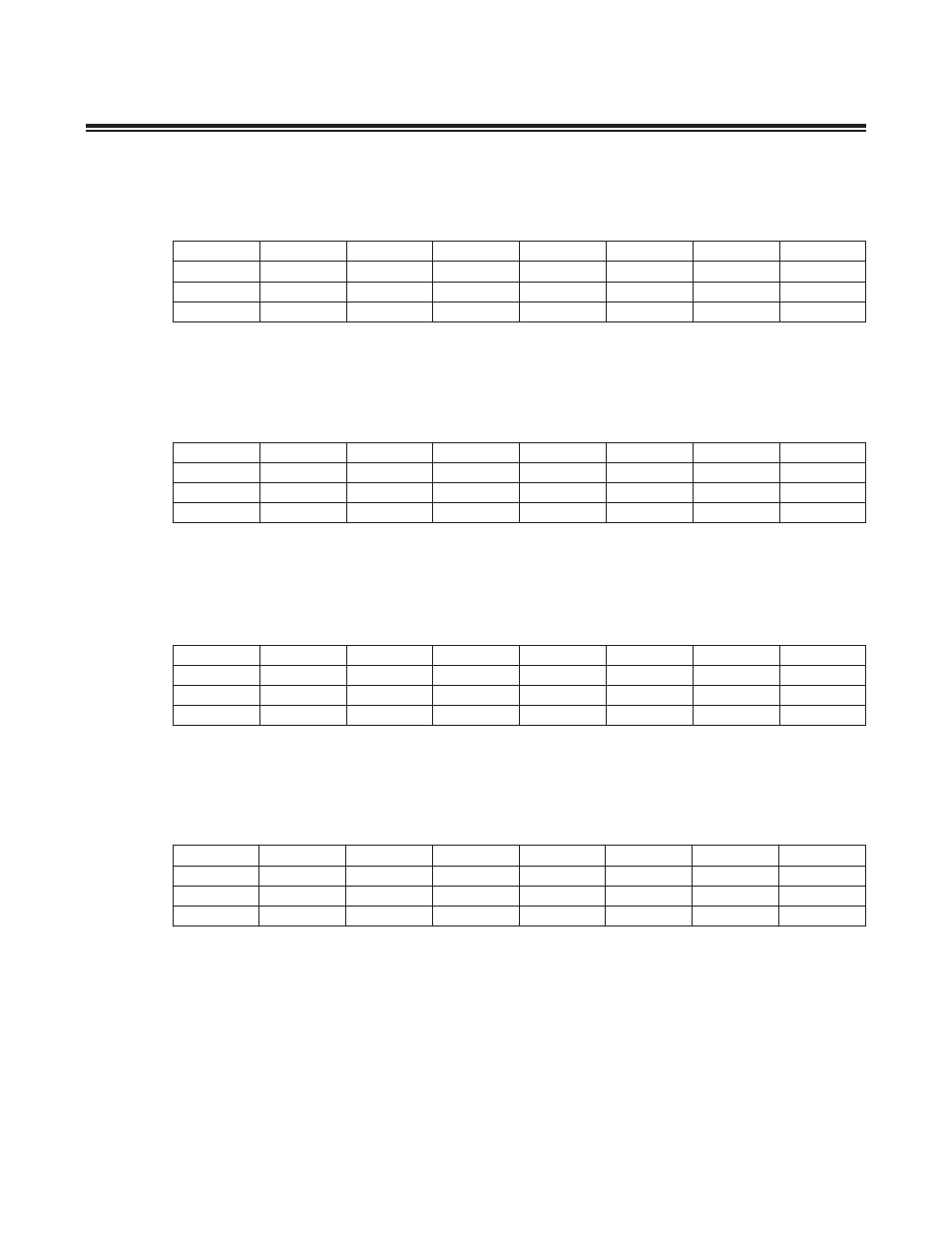
Bits 7:0: Port 4 Input Bits. The read values of these bits reflect the logic states present at port 4 pins P4 .0 to P4 .7 .
Bits 7:0: Port 5 Input Bits. The read values of these bits reflect the logic states present at port 5 pins P5 .0 to P5 .7 .
Bits 7:0: Port 6 Input Bits. The read values of these bits reflect the logic states present at port 6 pins P6 .0 to P6 .5 .
Bits 7:0: Input/Output Direction for Port 0. The bits in this register control the input/output direction for port pins P0 .0
to P0 .7 . When PD0 .n is set to 0, the corresponding port pin (P0 .n) acts as an input with characteristics determined by
PO0 .n . When PD0 .n is set to 1, the port pin acts as an output, driving the output state given by PO0 .n .
Register Name
PI4
Register Description
Port 4 Input Register
Register Address
M1[08h]
Register Name
PI5
Register Description
Port 5 Input Register
Register Address
M1[09h]
Register Name
PI6
Register Description
Port 6 Input Register
Register Address
M1[0Ah]
Bit #
7
6
5
4
3
2
1
0
Name
PI4 .7
PI4 .6
PI4 .5
PI4 .4
PI4 .3
PI4 .2
PI4 .1
PI4 .0
Reset
s
s
s
s
s
s
s
s
Access
r
r
r
r
r
r
r
r
Bit #
7
6
5
4
3
2
1
0
Name
PI5 .7
PI5 .6
PI5 .5
PI5 .4
PI5 .3
PI5 .2
PI54 .1
PI5 .0
Reset
s
s
s
s
s
s
s
s
Access
r
r
r
r
r
r
r
r
Bit #
7
6
5
4
3
2
1
0
Name
PI6 .7
PI6 .6
PI6 .5
PI6 .4
PI6 .3
PI6 .2
PI64 .1
PI6 .0
Reset
s
s
s
s
s
s
s
s
Access
r
r
r
r
r
r
r
r
Register Name
PD0
Register Description
Port 0 Direction Register
Register Address
M0[10h]
Bit #
7
6
5
4
3
2
1
0
Name
PD0 .7
PD0 .6
PD0 .5
PD0 .4
PD0 .3
PD0 .2
PD0 .1
PD0 .0
Reset
s
s
s
s
s
s
s
s
Access
rw
rw
rw
rw
rw
rw
rw
rw