2 usb data register (udata), 4 usb sie internal register descriptions, 1 function address register (fnaddr) – Maxim Integrated MAXQ622 User Manual
Page 175: 12 .3 .2 usb data register (udata) -5, 12 .4 usb sie internal register descriptions -5, 12 .4 .1 function address register (fnaddr) -5
MAXQ612/MAXQ622 User’s Guide
Maxim Integrated
12-5
Note: Writes to this register are ignored when UBUSY = 1.
12.3.2 USB Data Register (UDATA)
This register is used for supplying data for supported USB register write operation request and for returning data for
USB register read operation .
Bits 7 to 0: USB Data Register (UDATA[7:0]). These data register bits are used for supplying data for supported USB
register write operation request and for returning data for USB register read operation .
12.4 USB SIE Internal Register Descriptions
The internal control and data registers are accessed through the UADDR and UDATA registers as previously described .
These internal registers control all aspects of the SIE .
12.4.1 Function Address Register (FNADDR)
Note: Read access only when USBEN = 1. Reading the function address before USBEN = 1 can compromise USB functionality.
Bit 7: Reserved. Reads returns zero.
Bits 6 to 0: USB Register Address (FNADDR[6:0]). These register bits represent a unique value that identifies the
USB function . Upon reset and power-up, the address bits are defaulted to zero and are set by host during the enumera-
tion process . The address zero is reserved as the default value and cannot be assigned to any function . This register
also is cleared to 00h by a USB bus reset . The SIE updates this register after receiving the ACK handshake at the
conclusion of a Set_Address request from the host .
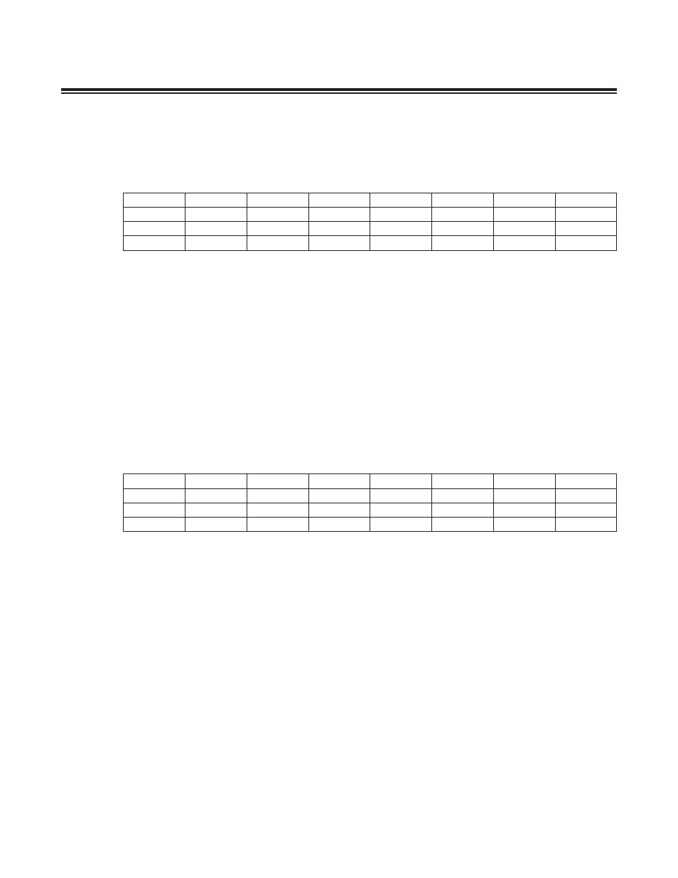
Register Name
UDATA
Register Description
USB Data Register
Register Address
M4[05h]
Register Name
FNADDR
Register Description
Function Address Register
Register Address
UADDR[4:0] = 01h
Bit #
7
6
5
4
3
2
1
0
Name
UDATA7
UDATA6
UDATA5
UDATA4
UDATA3
UDATA2
UDATA1
UDATA0
Reset
0
0
0
0
0
0
0
0
Access
rw
rw
rw
rw
rw
rw
rw
rw
Bit #
7
6
5
4
3
2
1
0
Name
—
FNADDR6
FNADDR5
FNADDR4
FNADDR3
FNADDR2
FNADDR1
FNADDR0
Reset
0
0
0
0
0
0
0
0
Access
r
r
r
r
r
r
r
r