Maxim Integrated MAXQ622 User Manual
Page 68
MAXQ612/MAXQ622 User’s Guide
4-12
Maxim Integrated
REGISTER
DESCRIPTION
ULDR, 08h[0Ch]
User Loader Starting Page Address (16 bits)
Initialization
This register is reset to the first page address past the available flash program memory on
all resets . On a part with 64KB of program memory with 512-byte pages, this register is
reset to 0080h .
Access
This register can only be modified when PRIV = HIGH . Unrestricted read access .
ULDR.8 to ULDR.0
User Loader Starting Page Address. These bits define the starting page address of the
user loader memory area .
ULDR.15 to ULDR.9
Reserved . Reads return 0 .
UAPP, 08h[0Dh]
User Application Starting Page Address (16 bits)
Initialization
This register is reset to the first page address past the available flash program memory on
all resets . On a part with 64KB of program memory with 512-byte pages, this register is
reset to 0080h .
Access
This register can only be modified when PRIV R MEDIUM . Unrestricted read access .
UAPP.8 to UAPP.0
User Application Starting Page Address. These bits define the starting page address of
the user application memory area .
UAPP.15 to UAPP.9
Reserved . Reads return 0 .
CKCN, 08h[0Eh]
System Clock Control Register (8 bits)
Initialization
Bits 4:0 are cleared to zero on all forms of reset . See bit description for bits 7:5 .
Access
Unrestricted read/write, except there is a locking mechanism for the PMME, CD1, and CD0
bits when changing their bits values; bit 5 is read-only .
CKCN.0 (CD0)
Clock Divide Bit 0
CKCN.1 (CD1)
Clock Divide Bit 1. If the PMME bit is cleared, the CD0 and CD1 bits control the number
of oscillator clocks required to generate one system clock as follows:
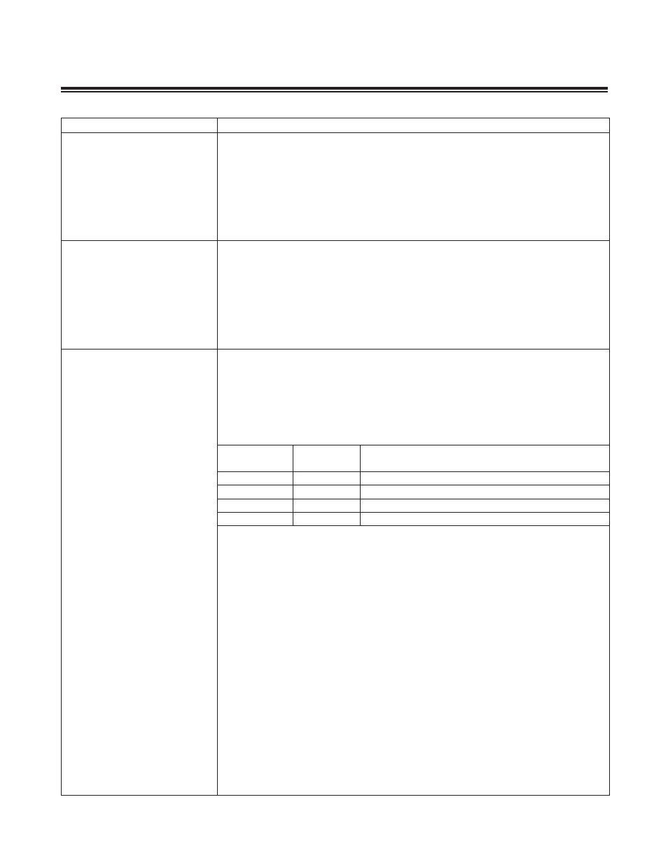
CD1
CD0
OSCILLATOR CLOCK CYCLES PER SYSTEM CLOCK
CYCLE
0
0
1 (default)
0
1
2
1
0
4
1
1
8
If the PMME bit is set to 1, the values of CD0 and CD1 cannot be altered and do not affect
the system clock frequency .
CKCN.2 (PMME)
Power-Management Mode Enable. If the PMME bit is cleared to 0, the values of CD0 and
CD1 determine the number of oscillator clock cycles per system clock cycle . If the PMME
bit is set to 1, the values of CD0 and CD1 are ignored and the system clock operates in a
fixed mode of 1 cycle per 256 oscillator cycles (divide by 256) .
If the PMME bit is set to 1, switchback mode has been enabled by setting the SWB bit and
a switchback source (such as an enabled external interrupt) is currently active, PMME is
cleared to 0 and cannot be set to 1 unless all switchback sources are inactive .
CKCN.3 (SWB)
Switchback Enable. If the SWB bit is cleared to 0, switchback mode is not active . If the
SWB bit is set to 1, switchback mode is active .
Switchback mode has no effect if power management mode is not active (PMME = 0) .
If power management mode is active and switchback mode is enabled, the PMME bit is
cleared to 0 when one of the qualifying events occurs . For details, refer to the switchback
description .
When any of these conditions cause switchback to clear PMME to 0, the system clock rate
is then determined by the settings of CD0 and CD1 . After PMME is cleared to 0 by switch-
back, it cannot be set back to 1 as long as any of the above conditions are true .
CKCN.4 (STOP)
Stop Mode Select. Setting this bit to 1 causes the MAXQ612/MAXQ622 to enter stop
mode . This does not change the currently selected clock divide ratio (CD0, CD1, PMME) .
CKCN.7 to CKCN.5
Reserved . Reads return 0 .