9 control of serial interface – Epson S1C88650 User Manual
Page 83
S1C88650 TECHNICAL MANUAL
EPSON
75
5 PERIPHERAL CIRCUITS AND THEIR OPERATION (Serial Interface)
5.8.9 Control of serial interface
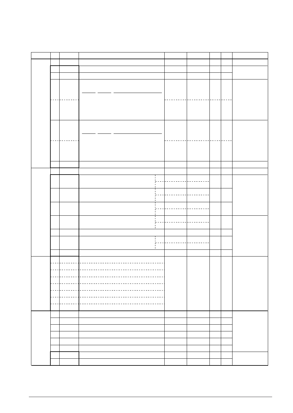
Table 5.8.9.1 show the serial interface control bits.
Table 5.8.9.1(a) Serial interface control bits
00FF48 D7
D6
D5
D4
D3
D2
D1
D0
–
EPR
PMD
SCS1
SCS0
SMD1
SMD0
ESIF
"0" when being read
Only for
asynchronous mode
In the clock synchro-
nous slave mode,
external clock is
selected.
–
0
0
0
0
0
0
0
R/W
R/W
R/W
R/W
R/W
R/W
R/W
–
With parity
Odd
Serial I/F
–
Non parity
Even
I/O port
SCS1
1
1
0
0
SCS0
1
0
1
0
Clock source
Programmable timer
f
OSC3
/ 4
f
OSC3
/ 8
f
OSC3
/ 16
SMD1
1
1
0
0
SMD0
1
0
1
0
Mode
Asynchronous 8-bit
Asynchronous 7-bit
Clock synchronous slave
Clock synchronous master
–
Parity enable register
Parity mode selection
Clock source selection
Serial I/F mode selection
Serial I/F enable register
00FF49 D7
D6
D5
D4
D3
D2
D1
D0
–
FER
PER
OER
RXTRG
RXEN
TXTRG
TXEN
–
Serial I/F framing error flag
Serial I/F parity error flag
Serial I/F overrun error flag
Serial I/F receive trigger/status
Serial I/F receive enable
Serial I/F transmit trigger/status
Serial I/F transmit enable
"0" when being read
Only for
asynchronous mode
–
0
0
0
0
0
0
0
R/W
R/W
R/W
R/W
R/W
R/W
R/W
–
No error
No operation
No error
No operation
No error
No operation
Stop
No operation
Disable
Stop
No operation
Disable
R
W
R
W
R
W
R
W
R
W
–
Error
Reset (0)
Error
Reset (0)
Error
Reset (0)
Run
Trigger
Enable
Run
Trigger
Enable
Address Bit
Name
SR R/W
Function
Comment
1
0
00FF4A D7
D6
D5
D4
D3
D2
D1
D0
TRXD7
TRXD6
TRXD5
TRXD4
TRXD3
TRXD2
TRXD1
TRXD0
X
R/W
High
Low
Serial I/F transmit/Receive data D7 (MSB)
Serial I/F transmit/Receive data D6
Serial I/F transmit/Receive data D5
Serial I/F transmit/Receive data D4
Serial I/F transmit/Receive data D3
Serial I/F transmit/Receive data D2
Serial I/F transmit/Receive data D1
Serial I/F transmit/Receive data D0 (LSB)
00FF4B D7
D6
D5
D4
D3
D2
D1
D0
–
–
–
–
–
–
STPB
SDP
Constantly "0" when
being read
–
–
–
–
–
–
0
0
R/W
R/W
–
–
–
–
–
–
Serial I/F stop bit selection
Serial I/F data input/output permutation selection
–
–
–
–
–
–
2 bits
MSB first
–
–
–
–
–
–
1 bit
LSB first