4 osc3 oscillation circuit, 5 switching the cpu clocks – Epson S1C88650 User Manual
Page 50

42
EPSON
S1C88650 TECHNICAL MANUAL
5 PERIPHERAL CIRCUITS AND THEIR OPERATION (Oscillation Circuits)
5.4.4 OSC3 oscillation circuit
The OSC3 oscillation circuit generates the system
clock when the CPU and some peripheral circuits
are in high speed operation.
This oscillation circuit stops when the SLP instruc-
tion is executed, or the SOSC3 register is set to "0".
In terms of oscillation circuit types, any one of
crystal oscillation, ceramic oscillation or CR
oscillation can be selected with the mask option.
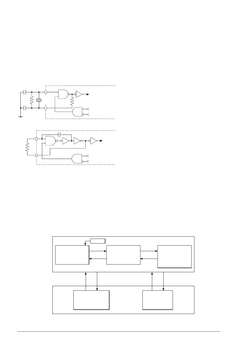
Figure 5.4.4.1 shows the configuration of the OSC3
oscillation circuit.
When CR oscillation is selected, the CR oscillation
circuit (Max. 2.2 MHz) is formed merely by
connecting a resistor (R
CR3
) between OSC3 and
OSC4 terminals.
5.4.5 Switching the CPU clocks
You can use either OSC1 or OSC3 as the system
clock for the CPU and you can switch over by
means of software.
You can save power by turning the OSC3 oscilla-
tion circuit off while the CPU is operating in OSC1.
When you must operate on OSC3, you can change
to high speed operation by turning the OSC3
oscillation circuit ON and switching over the
system clock.
In this case, since several msec to several tens of
msec are necessary for the oscillation to stabilize
after turning the OSC3 oscillation circuit ON, you
should switch over the clock after stabilization time
has elapsed.
When switching over from the OSC3 to the OSC1,
turn the OSC3 oscillation circuit OFF immediately
following the clock changeover.
When switching the system clock from OSC3 to
OSC1 immediately after the power is turned on, it
is necessary to wait for the OSC1 oscillation to
stabilize before the clock can be switched. The
OSC3 oscillation may take several tens of msec to
several seconds until it has completely stabilized.
(The oscillation start time will vary somewhat
depending on the oscillator and on the externally
attached parts. Refer to the oscillation start time
example indicated in Chapter 8, "ELECTRICAL
CHARACTERISTICS".)
Figure 5.4.5.1 indicates the status transition dia-
gram for the clock changeover.
V
SS
OSC4
OSC3
Rf
C
D2
C
G2
f
OSC3
Oscillation circuit
control signal
SLEEP status
X'tal 2
or
Ceramic
f
OSC3
Oscillation circuit
control signal
SLEEP status
OSC4
OSC3
R
CR3
(1) Crystal/Ceramic oscillation circuit
(2) CR oscillation circuit
Fig. 5.4.4.1 OSC3 oscillation circuit
When crystal or ceramic oscillation circuit is
selected, the crystal or ceramic oscillation circuit
(Max. 8.2 MHz) are formed by connecting either a
crystal oscillator (X'tal2) or a combination of
ceramic oscillator (Ceramic) and feedback resistor
(Rf) between OSC3 and OSC4 terminals and
connecting two capacitors (C
G2
, C
D2
) between the
OSC3 terminal and V
SS
, and between the OSC4
terminal and V
SS
, respectively.
RESET
SOSC3=1
SOSC3=0
CLKCHG=1
CLKCHG=0
ON
ON or OFF
STOP
HALT status
OSC1
OSC3
CPU clock
OFF
OFF
STOP
SLEEP status
OSC1
OSC3
CPU clock
Program Execution Status
HALT instruction
SLP instruction
Interrupt
Interrupt
(Input interrupt)
Standby Status
*
*
ON
ON
OSC3
High speed operation
OSC1
OSC3
CPU clock
ON
ON
OSC1
Low speed operation
OSC1
OSC3
CPU clock
Low speed and
low power operation
ON
OFF
OSC1
OSC1
OSC3
CPU clock
*
The return destination from the standby status becomes the program execution status prior to shifting to the standby status.
Fig. 5.4.5.1 Status transition diagram for the clock changeover
