2 power supply, 1 operating voltage, 2 internal power supply circuit – Epson S1C88650 User Manual
Page 15

S1C88650 TECHNICAL MANUAL
EPSON
7
2 POWER SUPPLY
2 POWER SUPPLY
In this section, we will explain the operating voltage and the configuration of the internal power
supply circuit of the S1C88650.
2.1 Operating Voltage
The S1C88650 operating power voltage is as
follows:
1.8 V to 3.6 V
2.2 Internal Power Supply Circuit
The S1C88650 incorporates the power supply
circuit shown in Figure 2.2.1. When voltage within
the range described above is supplied to V
DD
(+)
and V
SS
(GND), all the voltages needed for the
internal circuit are generated internally in the IC.
Roughly speaking, the power supply circuit is
divided into three sections.
Table 2.2.1 Power supply circuit
Circuit
Oscillation circuits,
Internal circuits
LCD system voltage
regulator
LCD driver
Power supply circuit
Internal logic
voltage regulator
Power voltage
booster
LCD system voltage
regulator
Output voltage
V
D1
V
DD
or
V
D2
V
C1
–
V
C5
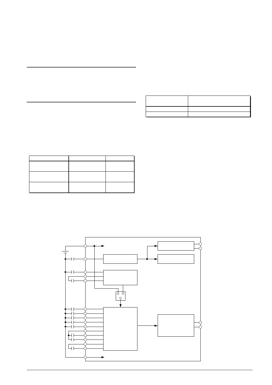
The internal logic voltage regulator generates the D1 > for driving the internal logic circuits and the oscillation circuit. D1 voltage value is fixed at 1.8 V (Typ.). The power voltage booster generates the operating D2 > for the LCD system voltage regulator. Either DD > or D2 > can be selected as the power source for the LCD system voltage regulator DD > power supply voltage level. Table 2.2.2 Power source for LCD system voltage regulator Supply voltage V DD 1.8–2.5 V Power source for LCD system voltage regulator V D2 V DD The V D2 voltage is about double the V DD voltage level. Refer to Chapter 8, "ELECTRICAL The LCD system voltage regulator generates the 1/ C1 >, C2 >, C3 >, C4 > and C5 >. See Chapter 8, "ELECTRICAL CHARACTERISTICS" for the voltage values. In the S1C88650, the LCD drive voltage is supplied Notes: • Under no circumstances should V D1 ,V D2 , V C1 , V C2 , V C3 , V C4 and V C5 , terminal output be used to drive external circuit. • If V DD is used as the power source for the LCD system voltage regulator when V DD is 2.5 V or less, the V C1 to V C5 voltages cannot be generated within specifications. V DD V D1 V D2 CF CG V C1 V C2 V C3 V C4 V C5 CA CC CE V SS Internal logic voltage regulator LCD system voltage regulator Oscillation circuit LCD driver V D1 V C1– V C5 Power voltage booster External OSC1, OSC2 COM0–COM31 Internal circuit V D2 Fig. 2.2.1 Configuration of power supply circuit
operating voltage
The V
voltage
according to the
2.5–3.6 V
CHARACTERISTICS", for details.
5-bias LCD drive voltages
to the built-in LCD driver which drives the LCD
panel connected to the SEG and COM terminals.
CB
CD
power
supply
OSC3, OSC4
SEG0–SEG125
