7 basic external wiring diagram, Panel, Recommended values for external parts – Epson S1C88650 User Manual
Page 147
S1C88650 TECHNICAL MANUAL
EPSON
139
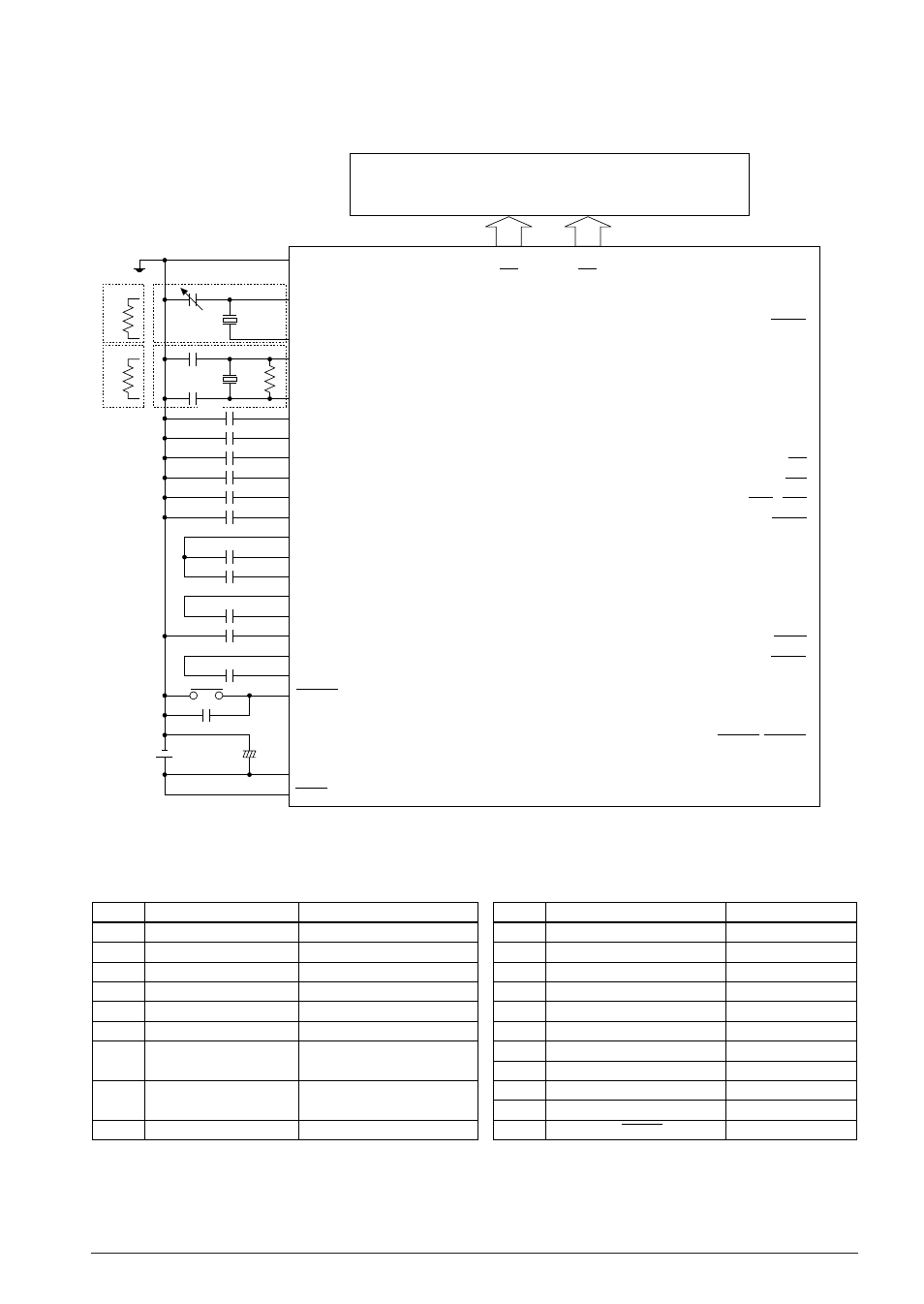
7 BASIC EXTERNAL WIRING DIAGRAM
7 BASIC EXTERNAL WIRING DIAGRAM
Note: The above table is simply an example, and is not guaranteed to work.
∗
1: OSC1 = Crystal oscillation
∗
2: OSC1 = CR oscillation
∗
3: OSC3 = Crystal or Ceramic oscillation
∗
4: OSC3 = CR oscillation
K00–K02
K03 (BREQ)
K04–K07
R00–R07 (A0–A7)
R10–R17 (A8–A15)
R20–R23 (A16–A19)
R24 (RD)
R25 (WR)
R30–R32 (CE0–CE2)
R33 (BACK)
P00–P07 (D0–D7)
P10 (SIN)
P11 (SOUT)
P12 (SCLK)
P13 (SRDY)
P14 (TOUT0/TOUT1)
P15 (TOUT2/TOUT3)
P16 (FOUT)
P17 (TOUT2/TOUT3)
Symbol
X'tal1
C
G1
R
CR1
X'tal2
Ceramic
Rf
C
G2
C
D2
R
CR3
Name
Crystal oscillator
Trimmer capacitor
Resistor for CR oscillation
Crystal oscillator
Ceramic oscillator
Feedback resistor
Gate capacitor
Drain capacitor
Resistor for CR oscillation
Recommended value
32.768 kHz, CI(Max.) = 35 k
Ω
0–25 pF
1.5 M
Ω
4 MHz
4 MHz
1 M
Ω
15 pF (Crystal oscillation)
30 pF (Ceramic oscillation)
15 pF (Crystal oscillation)
30 pF (Ceramic oscillation)
40 k
Ω
Recommended values for external parts
Symbol
C
1
C
2
C
3
C
4
C
5
C
6
C
7
–C
9
C
10
C
11
C
P
Cres
Name
Capacitor between V
SS
and V
D1
Capacitor between V
SS
and V
C1
Capacitor between V
SS
and V
C2
Capacitor between V
SS
and V
C3
Capacitor between V
SS
and V
C4
Capacitor between V
SS
and V
C5
Booster capacitors
Capacitor between V
SS
and V
D2
Booster capacitor
Capacitor for power supply
Capacitor for RESET terminal
Recommended value
0.1
µ
F
0.1
µ
F
0.1
µ
F
0.1
µ
F
0.1
µ
F
0.1
µ
F
0.1
µ
F
0.1
µ
F
0.1
µ
F
3.3
µ
F
0.47
µ
F
S1C88650
LCD
panel
126 x 32
[The potential of the substrate
(back of the chip) is V
SS
.]
V
SS
OSC1
OSC2
OSC3
OSC4
V
D1
V
C1
V
C2
V
C3
V
C4
V
C5
CA
CB
CC
CD
CE
V
D2
CF
CG
RESET
V
DD
TEST
C
G2
C
G1
C
1
C
2
C
3
C
4
C
5
C
6
C
7
C
8
C
9
C
10
C
11
X'tal1
Rf
Cres
3 V
C
P
+
-
SEG0
SEG125
COM0
COM31
X'tal2 or
Ceramic
R
CR3
R
CR1
C
D2
∗
2
∗
1
∗
3
∗
4