2 system controller and bus control, 1 bus mode and cpu mode settings, 2 address decoder (ce output) settings – Epson S1C88650 User Manual
Page 42
34
EPSON
S1C88650 TECHNICAL MANUAL
5 PERIPHERAL CIRCUITS AND THEIR OPERATION (System Controller and Bus Control)
5.2 System Controller and Bus Control
The system controller is a management unit which
sets such items as the bus mode in accordance with
memory system configuration factors.
For the purposes of controlling the system, the
following settings can be performed in software:
(1) Bus and CPU mode settings
(2)
____
Chip enable (CE) signal output settings
(3) WAIT state settings for external memory
(4) Page address setting of the stack pointer
Below is a description of the how these settings are
to be made.
5.2.1 Bus mode and CPU mode settings
The S1C88650 has two bus modes and two CPU
modes and the software must select appropriate
modes according to the external memory size
connected to the S1C88650.
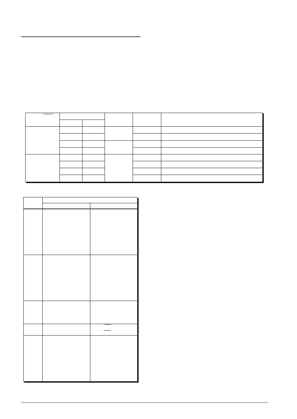
As shown in Table 5.2.1.1, these modes are speci-
fied usng the registers BUSMOD and CPUMOD.
Table 5.2.1.1 Bus and CPU mode settings
1
1
0
0
1
1
0
0
Expansion
Single chip
Expansion
Bus mode
Setting value
MCU/MPU
terminal
1 (MCU mode)
0 (MPU mode)
BUSMOD
Maximum
Minimum
Maximum
Minimum
Maximum
Minimum
Maximum
Minimum
CPU
mode
1
0
1
0
1
0
1
0
CPUMOD
Configuration of external memory
ROM+RAM
>
64K bytes (Program
≥
64K bytes)
ROM+RAM
>
64K bytes (Program
<
64K bytes)
None (Program
≥
64K bytes)
None (Program
<
64K bytes)
ROM+RAM
>
64K bytes (Program
≥
64K bytes)
ROM+RAM
>
64K bytes (Program
<
64K bytes)
ROM+RAM
>
64K bytes (Program
≥
64K bytes)
ROM+RAM
>
64K bytes (Program
<
64K bytes)
Table 5.2.1.2 I/O terminal settings
R00
R01
R02
R03
R04
R05
R06
R07
R10
R11
R12
R13
R14
R15
R16
R17
R20
R21
R22
R23
R24
R25
P00
P01
P02
P03
P04
P05
P06
P07
Output port R00
Output port R01
Output port R02
Output port R03
Output port R04
Output port R05
Output port R06
Output port R07
Output port R10
Output port R11
Output port R12
Output port R13
Output port R14
Output port R15
Output port R16
Output port R17
Output port R20
Output port R21
Output port R22
Output port R23
Output port R24
Output port R25
I/O port P00
I/O port P01
I/O port P02
I/O port P03
I/O port P04
I/O port P05
I/O port P06
I/O port P07
Single chip
Bus mode
Terminal
Expansion
Address bus A0
Address bus A1
Address bus A2
Address bus A3
Address bus A4
Address bus A5
Address bus A6
Address bus A7
Address bus A8
Address bus A9
Address bus A10
Address bus A11
Address bus A12
Address bus A13
Address bus A14
Address bus A15
Address bus A16
Address bus A17
Address bus A18
Address bus A19
RD signal
WR signal
Data bus D0
Data bus D1
Data bus D2
Data bus D3
Data bus D4
Data bus D5
Data bus D6
Data bus D7
The function of I/O terminals is set as shown in
Table 5.2.1.2 in accordance with mode selection.
At initial reset, the bus mode (CPU mode) is set as
explained below.
•
In MCU mode:
At initial reset, the S1C88650 is set in single chip
mode (minimum).
Accordingly, in MCU mode, even if a memory
has been externally expanded, the system is
activated by the program written to internal
ROM.
In the system with externally expanded
memory, perform the applicable bus mode
settings during the initialization routine
originating in internal ROM.
•
In MPU mode:
At initial reset, the S1C88650 is set in expansion
mode (minimum).
Therefore, the internal ROM will be disabled.
_____
5.2.2 Address decoder (CE output) settings
As explained in Section 3.6.4, the S1C88650 is
equipped with address decoders that can output a
_____ _____
maximum of three chip enable signals (CE0–CE2) to
external devices.