6 output ports (r ports), 1 configuration of output ports, 2 high impedance control – Epson S1C88650 User Manual
Page 59: 3 dc output
S1C88650 TECHNICAL MANUAL
EPSON
51
5 PERIPHERAL CIRCUITS AND THEIR OPERATION (Output Ports)
5.6 Output Ports (R ports)
5.6.1 Configuration of output ports
The S1C88650 is equipped with 26 bits of output
ports (R00–R07, R10–R17, R20–R25, R30–R33).
Depending on the bus mode setting, the configura-
tion of the output ports may vary as shown in the
table below.
Table 5.6.1.1 Configuration of output ports
Terminal
R00
R01
R02
R03
R04
R05
R06
R07
R10
R11
R12
R13
R14
R15
R16
R17
R20
R21
R22
R23
R24
R25
R30
R31
R32
R33
Bus mode
Expansion
Single chip
Address A0
Address A1
Address A2
Address A3
Address A4
Address A5
Address A6
Address A7
Address A8
Address A9
Address A10
Address A11
Address A12
Address A13
Address A14
Address A15
Address A16
Address A17
Address A18
Address A19
RD signal
WR signal
Output port R30/CE0 signal
Output port R31/CE1 signal
Output port R32/CE2 signal
Output port R33/BACK signal
Output port R00
Output port R01
Output port R02
Output port R03
Output port R04
Output port R05
Output port R06
Output port R07
Output port R10
Output port R11
Output port R12
Output port R13
Output port R14
Output port R15
Output port R16
Output port R17
Output port R20
Output port R21
Output port R22
Output port R23
Output port R24
Output port R25
Output port R30
Output port R31
Output port R32
Output port R33
Only the configuration of the output ports in single
chip mode will be discussed here. With respect to
bus control, see "5.2 System Controller and Bus
Control".
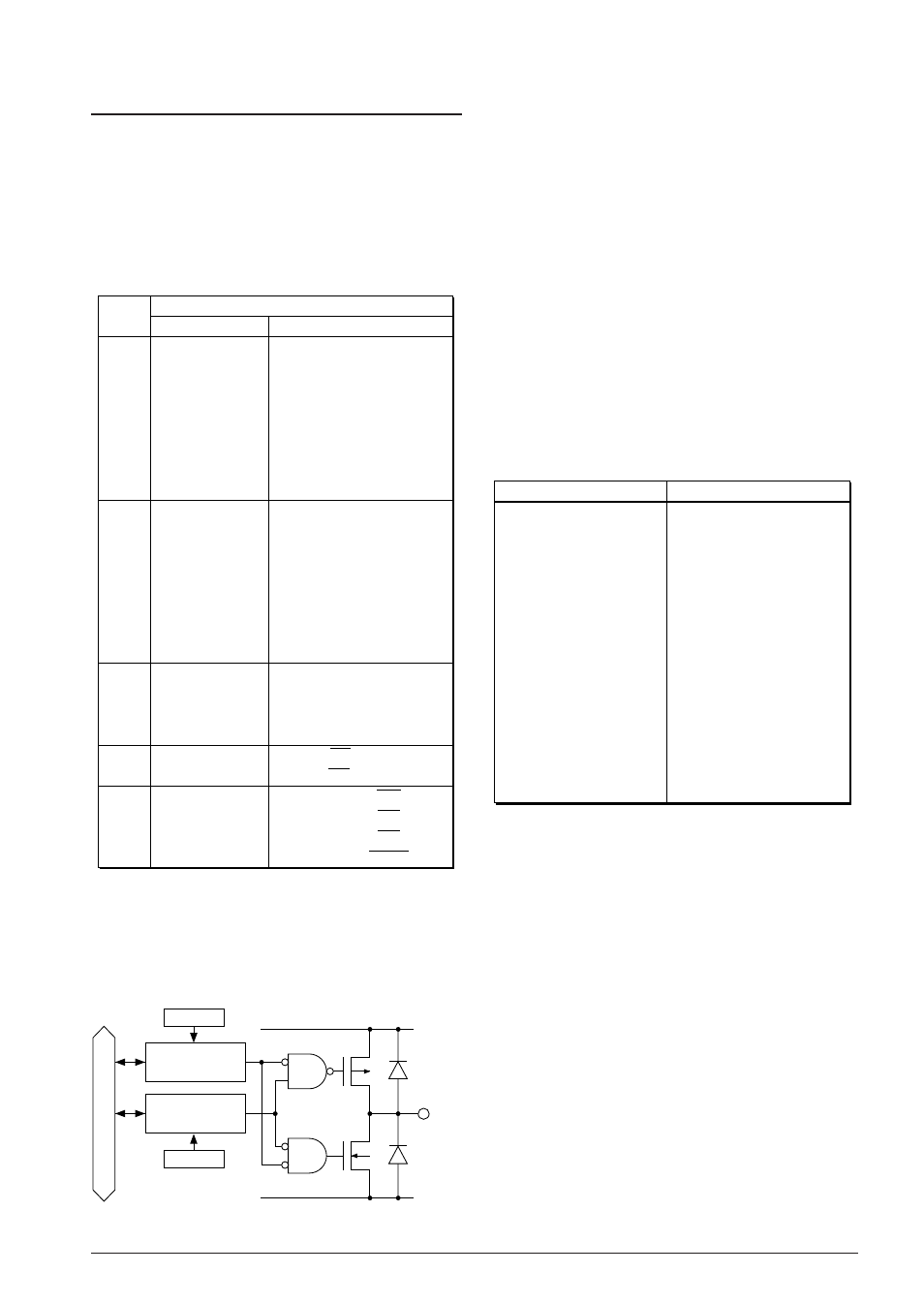
Figure 5.6.1.1 shows the basic structure of the
output ports.
V
DD
V
SS
Data bus
Rxx
Address
Data register
Address
High impedance
control register
Fig. 5.6.1.1 Structure of output ports
In expansion mode, the data registers and high
impedance control registers of the output ports
used for bus function can be used as general
purpose registers with read/write capabilities. This
will not in any way affect bus signal output.
The output specification of each output port is as
complementary output with high impedance
control in software possible.
5.6.2 High impedance control
The output port can be high impedance controlled
in software.
This makes it possible to share output signal lines
with an other external device.
A high impedance control register is set for each
series of output port terminals as shown below.
Either complementary output and high impedance
state can be selected with this register.
Table 5.6.2.1 High impedance control registers
Register
Output port terminal
HZR0L
HZR0H
HZR1L
HZR1H
HZR20
HZR21
HZR22
HZR23
HZR24
HZR25
HZR30
HZR31
HZR32
HZR33
R00–R03
R04–R07
R10–R13
R14–R17
R20
R21
R22
R23
R24
R25
R30
R31
R32
R33
When a high impedance control register HZRxx is
set to "1", the corresponding output port terminal
becomes high impedance state and when set to "0",
it becomes complementary output.
5.6.3 DC output
As Figure 5.6.1.1 shows, when "1" is written to the
output port data register, the output terminal
switches to HIGH (V
DD
) level and when "0" is
written it switches to LOW (V
SS
) level. When
output is in a high impedance state, the data
written to the data register is output from the
terminal at the instant when output is switched to
complementary.