7 control of lcd driver – Epson S1C88650 User Manual
Page 129
S1C88650 TECHNICAL MANUAL
EPSON
121
5 PERIPHERAL CIRCUITS AND THEIR OPERATION (LCD Driver)
5.11.7 Control of LCD driver
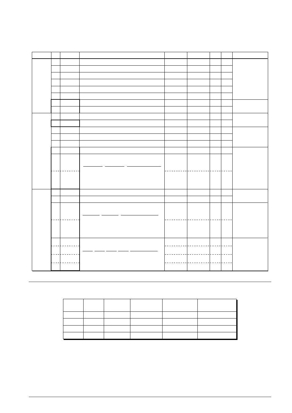
Table 5.11.7.1 shows the LCD driver control bits.
Table 5.11.7.1 LCD driver control bits
SR R/W
1
0
Address Bit
Name
Function
Comment
00FF03 D7
D6
D5
D4
D3
D2
D1
D0
–
–
–
–
–
–
0
0
R/W
R/W
–
–
–
–
–
–
Power source select for LCD voltage regulator
Power voltage booster On/Off control
Constantly "0" when
being read
–
–
–
–
–
–
V
D2
On
–
–
–
–
–
–
V
DD
Off
–
–
–
–
–
–
VDSEL
DBON
00FF10 D7
D6
D5
D4
D3
D2
D1
D0
HLMOD
SEGREV
–
–
–
DTFNT
LDUTY1
LDUTY0
Heavy load protection mode
Reverse SEG assignment
R/W register
R/W register
R/W register
LCD dot font selection
LCD drive duty selection
Reserved register
0
0
0
0
0
0
1
0
R/W
R/W
R/W
R/W
R/W
R/W
R/W
R/W
On
Reverse
1
1
1
12
×
12
Off
Normal
0
0
0
16
Ч
16/5
Ч
8
00FF11 D7
D6
D5
D4
D3
D2
D1
D0
FRMCS
DSPAR
LCDC1
LCDC0
LC3
LC2
LC1
LC0
LCD frame signal source clock selection
LCD contrast adjustment
These bits are reset
to (0, 0) when
SLP instruction
is executed.
0
0
0
0
0
0
0
0
R/W
R/W
R/W
R/W
R/W
R/W
R/W
R/W
PTM
f
OSC1
LCDC1
1
1
0
0
LCDC0
1
0
1
0
LCD display
All LCDs lit
All LCDs out
Normal display
Drive off
LDUTY1
1
1
0
0
LDUTY0
1
0
1
0
Duty
Not allowed
1/16
1/32
1/8
LC3
1
1
:
0
LC2
1
1
:
0
LC1
1
1
:
0
LC0
1
0
:
0
Contrast
Dark
:
:
Light
Display area 1 Display area 0
LCD display memory area selection
LCD display control
LDUTY0, LDUTY1: 00FF10H•D0, D1
Selects the drive duty.
Table 5.11.7.2 Setting drive duty
LDUTY1
1
1
0
0
LDUTY0
1
0
1
0
Duty
Not allowed
1/16
1/32
1/8
Common
terminal
–
COM0–COM15
COM0–COM31
COM0–COM7
Segment
terminal
–
SEG0–SEG125
SEG0–SEG125
SEG0–SEG125
Maximum number
of display dots
–
2,016 dots
4,032 dots
1,008 dots
At initial reset, LDUTY is set to "10" (1/16 duty).