Comtech EF Data DT-4500-A Series User Manual
Page 38
DT-4500A Series Downconverters
Revision 1
Introduction
MN-DT4500A
1–14
1.4.4
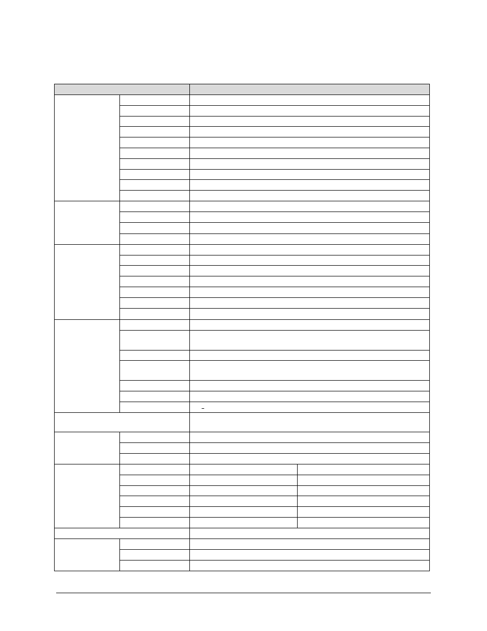
DT-4510-A, /D-A, DT-4511-A, DT-4512-A, /E -A K u-B and Downconverters
Characteristic
Specification
Frequency Range DT-4510-A
10.95-11.70 GHz
DT-4510D-A
10.70-11.70 GHz
DT-4511-A
11.70-12.20 GHz
DT-4512-A
12.20-12.75 GHz
DT-4512E-A
12.50-12.80 GHz
Conversion
Dual, No Inversion
Step Size
125 kHz standard, 1kHz optional
Preset Channels
32 Frequencies and Gains
Stability over Time
± 1 x 10
-9
/Day
Stability Over Temp
± 1 x 10
-8
0-50°C (32-122°F)
RF Input
Noise Figure
11 dB Maximum at 0 dB Attenuation
Level
-45 dBm Typical
Impedance
50Ω
Return Loss
20 dB min. with IO Module
IF Output
Output Level
+20 dBm at 1 dB Compression
Range
52-88 or 104-176 MHz
Intermodulation
-60 dBc @ 0 dBm Output SCL
Non-carrier Spurious -80 dBm
Carrier Spurious
-65 dBc @ 0 dBm Output
Return Loss
23 dB Minimum with IO Module
Impedance
50Ω or 75Ω
Transfer
Gain
45 dB ± 2 dB
Attenuation Adjust
0-20 in 0.25 dB Steps
0.1 dB Steps Optional
Gain Stability
± 0.25 dB/Day
Ripple
70MHz IFCF: ±0.25 dB (±18 MHz)
140 MHz IFCF: 0.75 dB (±36 MHz)
Slope
0.05 dB/MHz
Image Rejection
-80 dB Inband
AM to PM
0.1
o
. / dB for Output up to –5 dBm
External Reference
Input 5 or 10 MHz @ +3 dBm
Optional 10 MHz Rear Panel Reference Output
Group Delay
Linear Group Delay
0.03 ns/MHz
Parabolic Delay
0.01 ns/MHz
2
Group Delay Ripple
1.0 ns Peak-to-Peak
Phase Noise
Parameter
Limit (dBc/Hz)
Typical (dBc/Hz)
100 Hz
-72
-79
1 kHz
-79
-82
10 kHz
-89
-92
100 kHz
-98
-101
1 MHz
-110
-114
Remote Control (Rear Panel)
Comm Port EIA-485 or EIA-232
LED Indicators
(Front Panel)
Power On
Green LED
Receive
Yellow LED
Remote
Yellow LED