Altera JNEye User Manual
Page 149
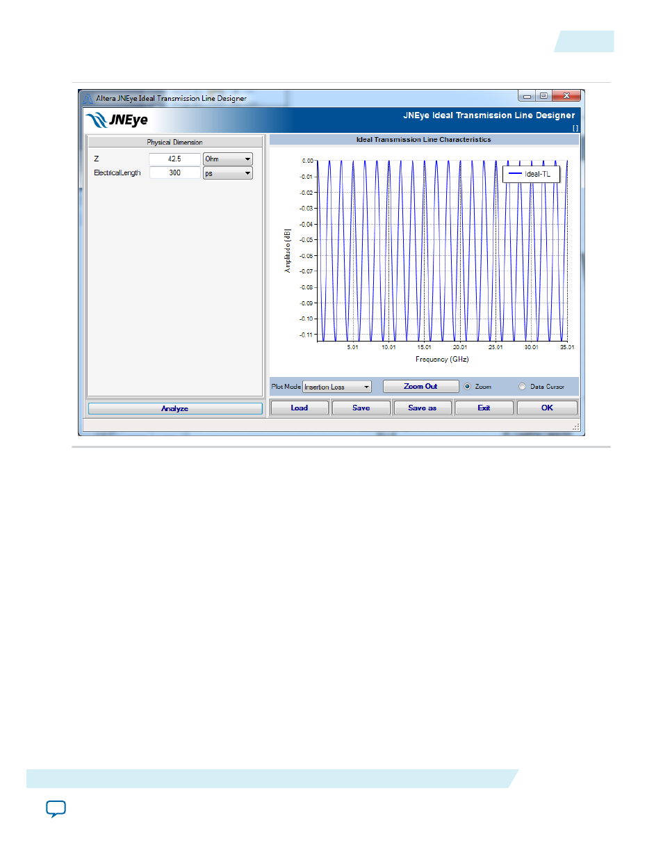
Figure 2-117: Ideal Transmission Line Channel Component Configuration
The channel component designer GUI can perform parameter unit conversion interactively. For example,
you can change the length unit from mil to mm and the GUI will automatically compute the length value
with the new unit.
After entering the model parameters, click Analyze and Channel Designer will compute the frequency
response of the current design. The integrated plotting engine can display the insertion loss or return
loss characteristics. When you alter the model parameters, the GUI displays a message that indicates the
channel characteristics may have changed. Click Analyze to redraw the channel characteristics. You can
also load or save the component design for reuse in the future.
If you are satisfied with your design, click OK to save and close the component design GUI. If you click
Exit or the X button of the window, the design will be discarded.
Via Component
In printed circuit board design, a via consists of two pads in corresponding positions on different layers of
the board. The pads are electrically connected by a hole through the board. In JNEye Channel Designer,
an analytical PCB Via model is constructed. A typical PCB via structure is shown in the following figure
UG-1146
2015.05.04
JNEye Channel Designer
2-143
Functional Description
Altera Corporation