Clock and reset signals, Clock and reset signals -12 – Altera Hybrid Memory Cube Controller User Manual
Page 49
Clock and Reset Signals
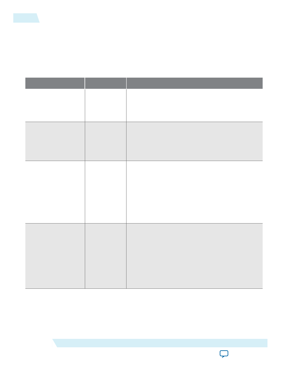
Table 4-7: HMC Controller IP Core Clock and Reset Signals
The HMC Controller IP core has a single clock domain outside of the transceiver. Your design must derive the
external TX PLL reference clock, the RX CDR reference clock, and the HMC device
REFCLKP
and
REFCLKN
input
reference clock signals from the same clock reference source.
Clock Name
Direction
Description
rst_n
Input
Active low master reset signal for the HMC Controller IP
core.
When asserted, the signal must remain asserted for at least
two
rx_cdr_refclk0
clock cycles.
core_rst_n
Output
When asserted, indicates that the HMC Controller IP core is
in reset.
The IP core deasserts the
core_rst_n
signal only after
core_clk
is stable and the transceiver is ready to transmit
data.
rx_cdr_refclk0
Input
Reference clock for the RX transceiver CDR PLL.
You must drive this clock with the frequency you specify for
the CDR reference clock parameter.
rx_cdr_refclk0
is not the reference clock for the TX PLL.
The reference clock for the TX PLL is an input to the
external TX PLL IP cores that you connect to your HMC
Controller IP core. The reference clock for the TX PLLs does
not drive the HMC Controller IP core directly.
tx_bonding_
clocks[95:0]
(for
full-width IP cores)
tx_bonding_
clocks[47:0]
(for
half-width IP cores)
Input
Clocks for the individual transceiver channels. The input
clock to each transceiver channel has six bits.
You must connect this input bus to a set of external
transceiver TX PLL IP cores. You must parameterize each
external TX PLL IP core to specify an output frequency that
is 1/2 the per-lane data rate. For a 10 Gbps HMC Controller
IP core lane rate, the TX PLL IP core output frequency must
be 5 GHz; for a 12.5 Gbps lane rate, the TX PLL IP core
output frequency must be 6.25 GHz.
4-12
Clock and Reset Signals
UG-01152
2015.05.04
Altera Corporation
HMC Controller IP Core Signals