Altera Hybrid Memory Cube Controller User Manual
Page 21
In the transceiver PLL parameter editor, you must follow the instructions in the Arria 10 Transceiver PHY
User Guide to configure the PLL IP core in the xN bonding configuration or in the PLL feedback
compensation bonding configuration. In addition, you must set the following parameter values:
• PLL output frequency to one half of the per-lane data rate of the IP core variation. The transceiver
performs dual edge clocking, using both the rising and falling edges of the input clock from the PLL.
Therefore, this PLL output frequency setting drives the transceiver with the correct clock for the lanes
that connect to the HMC device.
• PMA interface width to 32.
• PLL integer reference clock frequency (ATX PLL) or Desired reference clock frequency (fPLL)
depends on the bonding scheme.
• In the xN bonding scheme, Altera recommends that you specify one of 125 MHz, 156.25 MHz, or
166.67 MHz. You can theoretically specify any reference clock frequency from which the PLL can
generate the required output clock frequency. However, you must drive this TX PLL and the RX
CDR PLL (
rx_cdr_refclk0
input signal to the HMC Controller IP core) and the HMC device
reference clock input signals (
REFCLKP
and
REFCLKN
) from the same clock source.
• In the PLL feedback compensation bonding scheme, you must specify the lane rate divided by 32.
In this mode, the PLL is configured to bypass the reference clock divider. Therefore, if you select
this bonding scheme, the reference clock frequency must be the lane rate divided by the PMA
width, which is 32.
Note: You must drive the external PLL reference clock input signal at the frequency you specify for
this parameter.
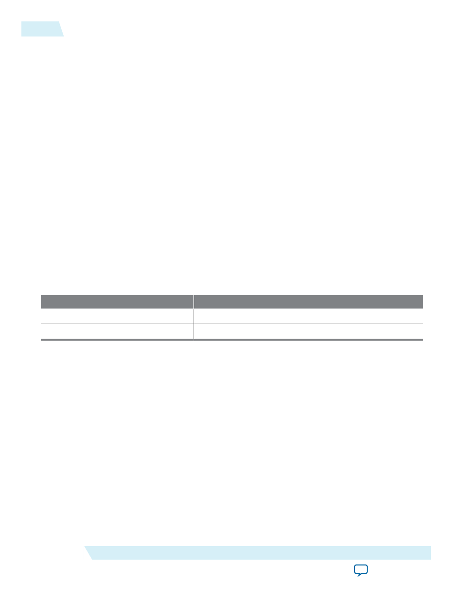
Table 2-4: Required PLL Reference Clock Frequency with PLL Feedback Compensation Bonding
Lane Rate
Required PLL Reference Clock Frequency
10 Gbps
312.5 MHz
12.5 Gbps
390.625 MHz
The number of external PLLs you must define depends on the bonding mode you specify. In xN bonding
mode, a single PLL is sufficient to drive the channels in the configured transceiver blocks. Recall that your
HMC link TX serial lanes must be configured in order in adjacent physical transceiver channels so that
these lanes configure a maximum of three transceiver blocks. You can view I/O constraints that enforce
these requirements in the example design Quartus Settings File
hmcc_example.qsf
provided with the HMC
Controller IP core.
You set the bonding mode in the PLL parameter editor. In PLL Feedback Compensation mode, each PLL
output connects to the x6 network for its transceiver block through the transceiver block's Master Clock
Generation Block. In xN bonding mode, the PLL output connects directly to the x6 network for its
transceiver block and drives additional transceiver blocks through the xN clock network.
2-12
Adding the External PLL
UG-01152
2015.05.04
Altera Corporation
Getting Started with the HMC Controller IP Core