Connector pinout of boards, Ice and jtag, Ethernet signal from or to phyceiver – Solvline Eddy DKV2.1.0.3 User Manual
Page 42
Chapter 3. Development
Environment
42
23
GND
24
3.3V
87
PC13
88
3.3V
25
P3_TX-
26
nRESET
89
3.3V
90
PC14
27
GND
28
3.3V
91
PC15
92
PC17
29
P4_RX+
30
RxD0#
93
PC18
94
PC19
31
3.3V
32
GND
95
PC24
96
PC20
33
P4_RX-
34
RTS0
97
NC
98
PC25
35
P4_TX+
36
TxD0#
99
I2C_TWCK
100 I2C_TWD
37
GND
38
CTS0
101 GND
102 GND
39
P4_TX-
40
3.3V
103 DDM
104 DDP
41
DEBUG_TxD
42
DSR0
105 DM2
106 DP2
43
DEBUG_RxD
44
RI0
107 DM3
108 DP3
45
PA5
46
RxD1#
109 DM4
110 DP4
47
PA22
48
RTS1
111 SDDATA0
112 SDDATA1
49
GND
50
GND
113 SDDATA2
114 GND
51
PA30
52
TxD1#
115 SDCMD
116 SDDATA3
53
NC
54
CTS1
117 SDCDN
118 SDCLK
55
GND
56
NRST
119 JTAG_SEL
120 SDWP
57
PB0
58
PB1
121 NC
122 BMS
59
PB2
60
PB3
123 NC
124 3.3V
61
PB12
62
GND
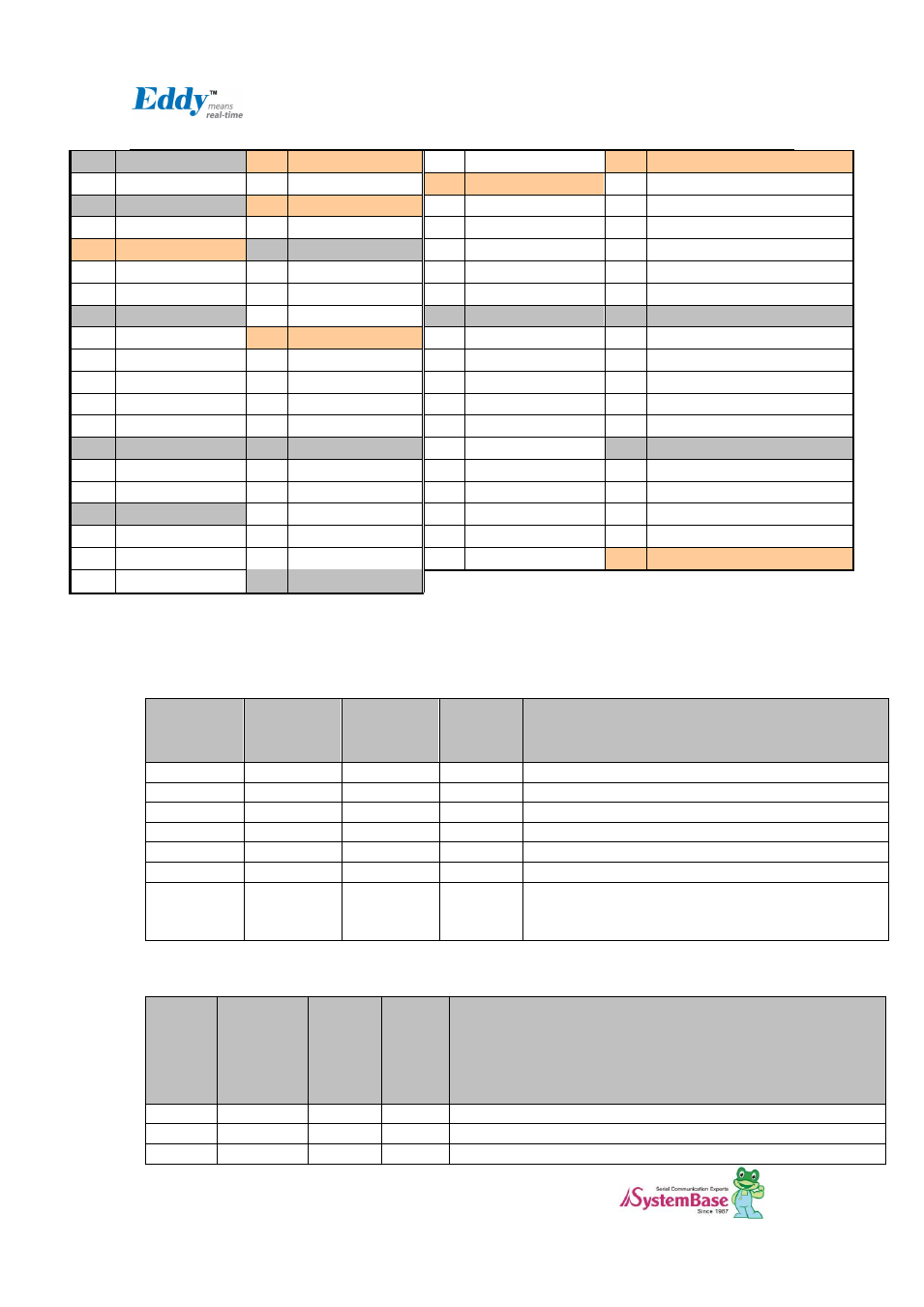
2.5.2
Connector Pinout of Boards
2.5.2.1. ICE and JTAG
S4M
Pin No
(124)
Name
S4M-JIG
Pin HDR
(46*2)
S4M-DK
Pin HDR
(46*2)
Description
1
TDI
-
-
Test Data IN
2
TDO
-
-
Test Data Out
3
TMS
-
-
Test Mode Select
4
RTCK
-
-
Return Test Clock
5
TCK
-
-
Test Clock
6
NTRST
-
-
Test Reset
119
JTAGSEL
-
-
JTAG boundary scan can be used by connecting J3.
This pin should not be connected when using ICE (In-Circuit
Emulator) or in normal operation status.
2.5.2.2. Ethernet signal from or to PHYceiver
S4M
Pin No
(124)
Name
S4M-JIG
Pin HDR
(46*2)
S4M-
DK
Pin
HDR
(46*2)
Description
7
LAN_RX+
J5 pin2
J7 Pn2
Ethernet PHY Physical receive or transmit signal (+ differential) in CPU
8
LAN_TX+
J5 pin1
J7 Pin1
Ethernet PHY Physical receive or transmit signal (- differential) in CPU
9
LAN_RX-
J5 pin3
J7 pin3
Ethernet PHY Physical receive or transmit signal (+ differential) in CPU