Solvline Eddy DKV2.1.0.3 User Manual
Page 18
Chapter 2. Getting Started
18
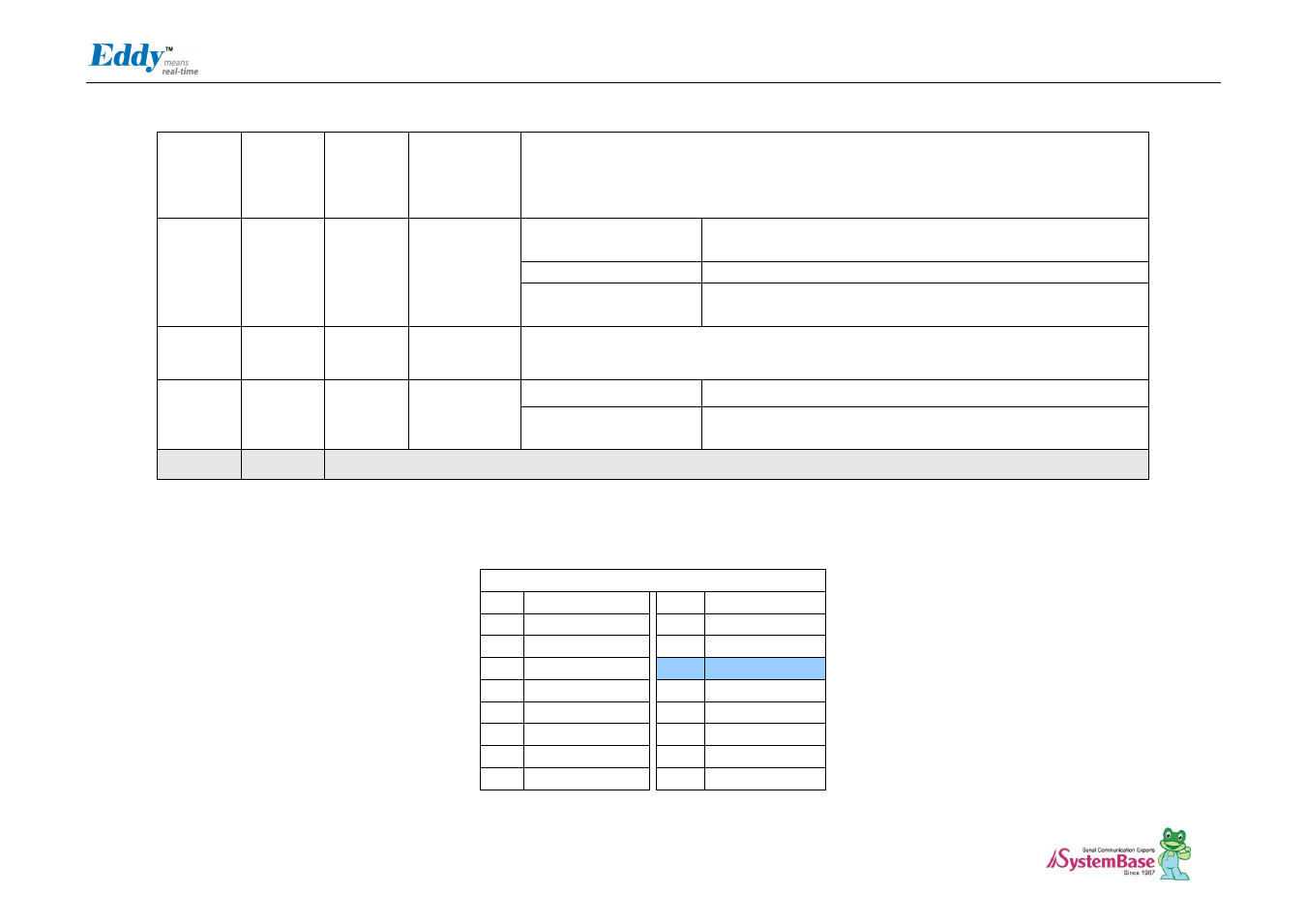
25~32
D[7:0]
J9_25
- J3_32
J3_29 - J3_36
External Data Bus 0-7
DK is directly connected with CPU and external connecter (J3) is connected by buffer. You
should enable PC13(NCS6 : Chip Select 6) for working buffer, if you reset, it becomes Pulled-up
input.
33
PC13
J9_33
J4_18
Edd-DK v2.1 : NCS6
Data Bus connected with external header can be used when NCS6
is enabled.
Peripheral A : FIQ
Fast Interrupt Input
Peripheral B : NCS6
External device Chip Select 6
256MB memory area addressable, active low
34
JTAGSEL
J9_34
-
JTAG boundary scan can be used by connecting pin34 and 36(J14 connection). This pin should
not be connected when using ICE (In-Circuit Emulator) or in normal operation status.
35
PC12
J9_35
J4_17
Peripheral A : IRQ0
External Interrupt Input 0
Peripheral B : NCS7
External device Chip Select 7.
256MB memory area addressable, active low
36
NC
Not Connect
J3 Specifications
J3
Pin
Signal Name
Pin
Signal Name
1
PID0
2
PID1
3
PID2
4
PID3
5
PID4
5
GND
7
PC14
8
PC17
9
PC18
10
PC8 (RTS3)
11
PC20
12
PC10 (CTS3)
13
PA22
14
PC15 (IRQ1)
15
PB8
16
PB9 (RXD2)