Solvline Eddy DKV2.1.0.3 User Manual
Page 17
Chapter 2. Getting Started
17
13
A3
14
A2
15
A1
16
A0
17
PC9
18
NWE
19
FPG
20
NRD
21
GND
22
3.3V
23
GND
24
3.3V
25
D7
26
D6
27
D5
28
D4
29
D3
30
D2
31
D1
32
D0
33
PC13
34
JTAGSEL
35
PC12
36
NC
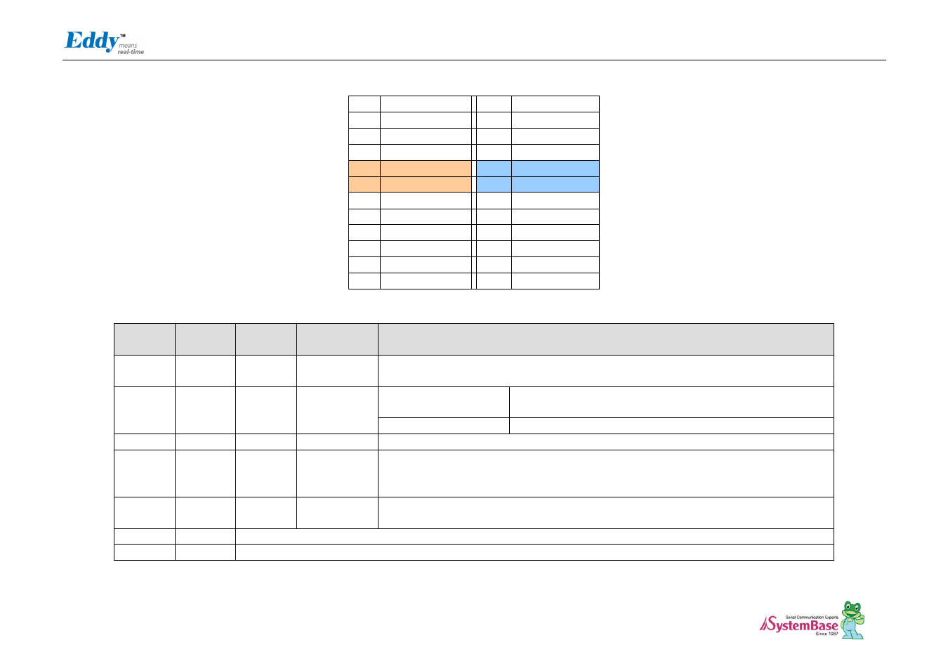
J2 Pin Description
Pin No
Name
DK v2.1
Pin No
Expansion
Header Pin No
Description
1~16
A[15:0]
J9_1
-J9_16
J3_4-J3_20
External Address Bus 0-15 (0 at reset)
DK is directly connected with CPU and external connecter (J3) is connected by buffer.
17
PC9
J9_17
J4_14
Peripheral A : NCS5
External device Chip Select 5.
256MB memory area addressable, active low
Peripheral B : TIOB0
Timer Counter ch0 I/O Line B
18
NEW
J9_18
J1_21
External device Write Enable signal, active low
19
FPG
J9_19
-
For Flash Programming
You can program Data Flash in Eddy CPU v2.1 via USB. Refer to 2.4.2.3 S6:NAND Flash & Data
Flash Chip Select for further information.
20
NRD
J9_20
J1_23
External device Read Enable signal, active low
21, 23
GND
Ground
22, 24
3.3V
3.0V to 3.6V power input