Solvline Eddy DKV2.1.0.3 User Manual
Page 19
Chapter 2. Getting Started
19
17
PB10
18
PB11(RXD3)
19
PC0
20
PC1 (AD1)
21
PC2
22
PC3 (AD3)
23
PB14 (DRXD)
24
PB15 (DTXD)
25
GND
26
GND
27
BMS
28
NRST
29
PB23 / DCD0
30
PB5 / RXD0
31
PB4 / TXD0
32
PB24 / DTR0
33
PB22 / DSR0
34
PB26 / RTS0
35
PB27 / CTS0
36
PB25 / RI0
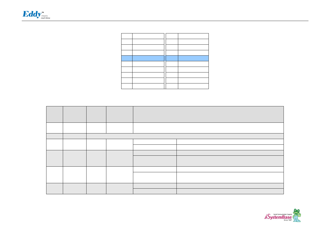
J3 Pin Description
Pin No
Name
DK v2.1
Pin No
Expansion
Header Pin
No
Description
1-5
PID[4:0]
J8_1
~J8_5
-
Product ID only used by the manufacturer.
Please do not work on these pins.
6,25,26
GND
Ground
7
PC14
J8_7
J4_19
Peripheral A : NCS3
External Device Chip Select 3
Peripheral B : IRQ2
External Interrupt Input 2
8
PC17
J8_8
J4_22
Peripheral A : D17
External Data Bus
Peripheral B :
SPI0_NPCS3
Disabled
9
PC18
J8_9
J4_23
Peripheral A : D18
External Data Bus
Peripheral B :
SPI1_NPCS1
SPI1(Serial Peripheral Interface) Peripheral Chip Select 1
10
PC8
J8_10
J4_13
Peripheral A : NCS4
External Device Chip Select 4
Peripheral B : RTS3
USART3 Request to Send