Additional design details, Shared spi bus with peripherals – Digilent 410-087P-KIT User Manual
Page 99
Spartan-3E Starter Kit Board User Guide
99
UG230 (v1.0) March 9, 2006
Additional Design Details
R
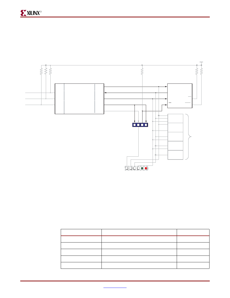
Additional Design Details
provides additional details of the SPI Flash interface used on the Spartan-3E
Starter Kit board. In most applications, this interface is as simple as that shown in
. The Spartan-3E Starter Kit board, however, supports of variety of
configuration options and demonstrates additional Spartan-3E capabilities.
Shared SPI Bus with Peripherals
After configuration, the SPI Flash configuration pins are available to the application. On
the Spartan-3E Starter Kit board, the SPI bus is shared by other SPI-capable peripheral
devices, as shown in
. To access the SPI Flash memory after configuration, the
FPGA application must disable the other devices on the shared PCI bus.
shows
the signal names and disable values for the other devices.
Figure 12-18:
Additional SPI Flash Interface Design Details
3.3V
(T4)
SPI_MOSI
(N10)
(U16)
(U3)
Spartan-3E FPGA
SPI_MISO
SPI_SCK
SPI_SS_B
D
C
Q
S
STMicro M25P16
SPI Serial Flash
CCLK
DIN/D0
MOSI/CSI_B
CSO_B
(R12)
Jumper J11
W
HLD
User-I/O
VS0/A19
VS1/A18
VS2/A17
SF_A<19>
(V15)
SF_A<18>
SF_A<17>
(U15)
(T16)
C
S
O_B
S
EL
S
EL
S
DI
S
DO
S
CK
GND
3
.3
V
ROM_C
S
C
S
O_B
Programming
Header J12
Other de
vice
s
s
h
a
re
S
PI
bu
s
DAC
AMP
ADC
Platform
Flash
Strata-
Flash
SPI_ALT_CS_JP11
UG230_c15_17_030306
Table 12-3:
Disable Other Devices on SPI Bus
Signal
Disabled Device
Disable Value
DAC_CS
Digital-to-Analog Converter (DAC)
1
AMP_CS
Programmable Pre-Amplifier
1
AD_CONV
Analog-to-Digital Converter (ADC)
0
SF_CE0
StrataFlash Parallel Flash PROM
1
FPGA_INIT_B
Platform Flash PROM
1