Ddr sdram connections – Digilent 410-087P-KIT User Manual
Page 104
104
Spartan-3E Starter Kit Board User Guide
UG230 (v1.0) March 9, 2006
Chapter 13: DDR SDRAM
R
The differential clock pin SD_CK_P is fed back into FPGA pin B9 in I/O Bank 0 to have best
access to one of the FPGA’s Digital Clock Managers (DCMs). This path is required when
using the MicroBlaze OPB DDR controller. The MicroBlaze OPB DDR SDRAM controller
IP core documentation is also available from within the EDK 8.1i development software
(see
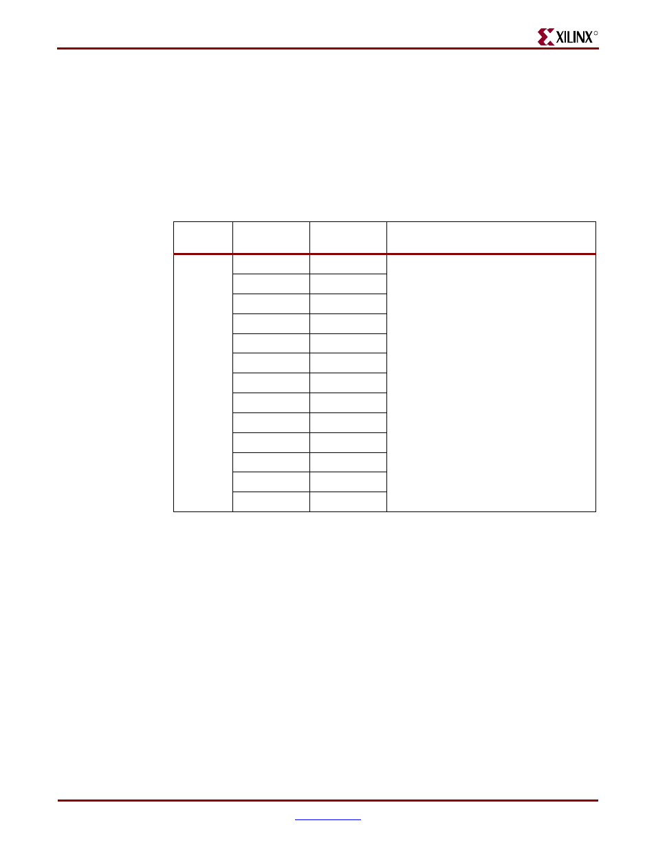
DDR SDRAM Connections
shows the connections between the FPGA and the DDR SDRAM.
Table 13-1:
FPGA-to-DDR SDRAM Connections
Category
DDR SDRAM
Signal Name
FPGA Pin
Number
Function
Ad
dr
ess
SD_A12
P2
Address inputs
SD_A11
N5
SD_A10
T2
SD_A9
N4
SD_A8
H2
SD_A7
H1
SD_A6
H3
SD_A5
H4
SD_A4
F4
SD_A3
P1
SD_A2
R2
SD_A1
R3
SD_A0
T1
See also other documents in the category Digilent Hardware:
- 410-282P-KIT (4 pages)
- 410-279P-KIT (26 pages)
- 410-258P-KIT (16 pages)
- 410-138P-KIT (28 pages)
- 410-178P-KIT (22 pages)
- 410-292P-KIT (29 pages)
- 410-274P-KIT (29 pages)
- 410-182P-KIT (22 pages)
- 410-134P-KIT (17 pages)
- 410-183P-KIT (19 pages)
- 410-155P-KIT (12 pages)
- 6015-410-001P-KIT (26 pages)
- 410-146P-KIT (4 pages)
- 6003-410-000P-KIT (138 pages)
- XUPV2P (23 pages)
- 410-047-C2P-KIT (3 pages)
- WaveForms (85 pages)
- 410-297P-KIT (25 pages)
- 410-295P-KIT (37 pages)
- 410-296P-KIT (23 pages)
- 410-209P-KIT REV.D (16 pages)
- 410-209P-KIT REV.C (17 pages)
- 410-254P-KIT (17 pages)
- 410-280P-KIT (9 pages)
- 410-202P-KIT (20 pages)
- 410-273P-KIT (24 pages)
- 410-269P-KIT (11 pages)
- 410-216P-KIT (15 pages)
- 410-231P-KIT (4 pages)
- 410-211P-KIT (10 pages)
- 410-262P-KIT (8 pages)
- 410-229P (7 pages)
- 410-242P-KIT (4 pages)
- 6021-210-000P-KIT (27 pages)
- 410-185P-KIT (21 pages)
- 6032-410-000P-BOARD (4 pages)
- 410-174P (17 pages)
- 410-145P (6 pages)
- 210-264P-BOARD (3 pages)
- 6003-210-012P (27 pages)
- 410-236P-BOARD (2 pages)
- 410-163P (1 page)
- 410-097P-KIT (2 pages)
- 410-255P-KIT (1 page)